没有合适的资源?快使用搜索试试~ 我知道了~
首页CC2640R2F-Q1蓝牙模块:汽车级低功耗MCU技术规格
CC2640R2F-Q1蓝牙模块:汽车级低功耗MCU技术规格
需积分: 26 2 下载量 96 浏览量
更新于2024-07-15
收藏 2.5MB PDF 举报
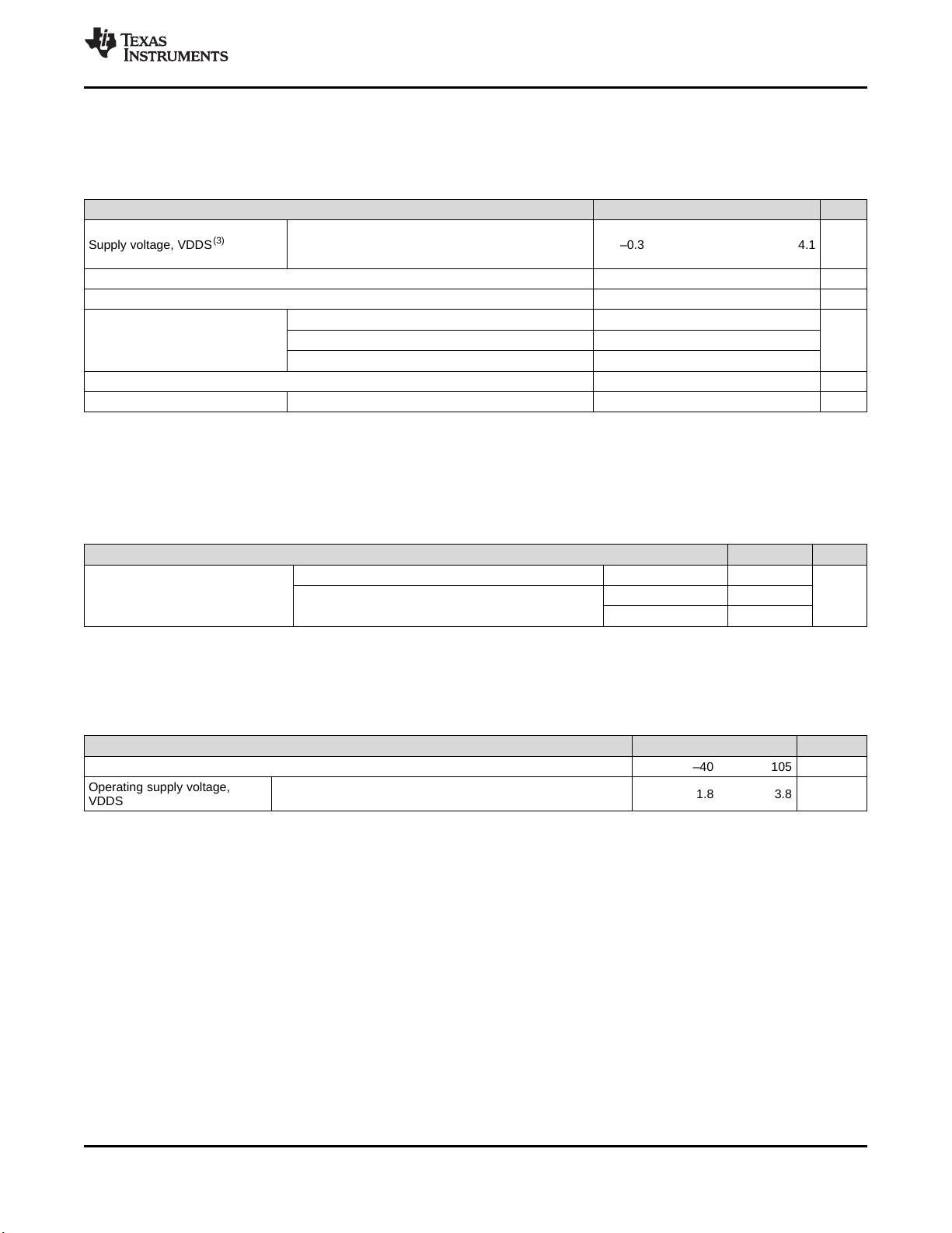
"CC2640R2F-Q1是一款专为汽车应用设计的低功耗蓝牙MCU,它由TI公司提供,满足严格的AEC-Q100标准,确保在极端的-40℃至+105℃温度范围内稳定工作。这款产品具有高度的可靠性和安全性,包括: 1. 核心处理器:基于ARM Cortex-M3架构,具有高性能,EEMBC CoreMark评分高达142分,能实现48MHz的时钟速度,内置275KB非易失性存储器,其中包含128KB系统可编程闪存,以及28KB系统SRAM,其中20KB为超低泄漏SRAM,支持8KB SRAM作为缓存或系统RAM。 2. 低功耗传感器控制器:独立于主系统运行,采用16位架构,配备2KB超低泄漏电流代码和数据SRAM,有助于延长电池寿命,特别适合对能耗敏感的应用。 3. 无线升级能力:支持无线固件更新(Over-the-Air, OTA),便于后期维护和功能扩展。 4. 封装和尺寸:汽车级封装,采用7mm×7mm RGZVQFN48封装,侧面具备湿可焊性,方便集成。 5. 丰富的外设接口:31个通用GPIO引脚,可灵活配置;四个通用定时器模块,支持PWM;并配备一个12位ADC,采样速率为200ksps,具有8通道模拟多路复用功能。 
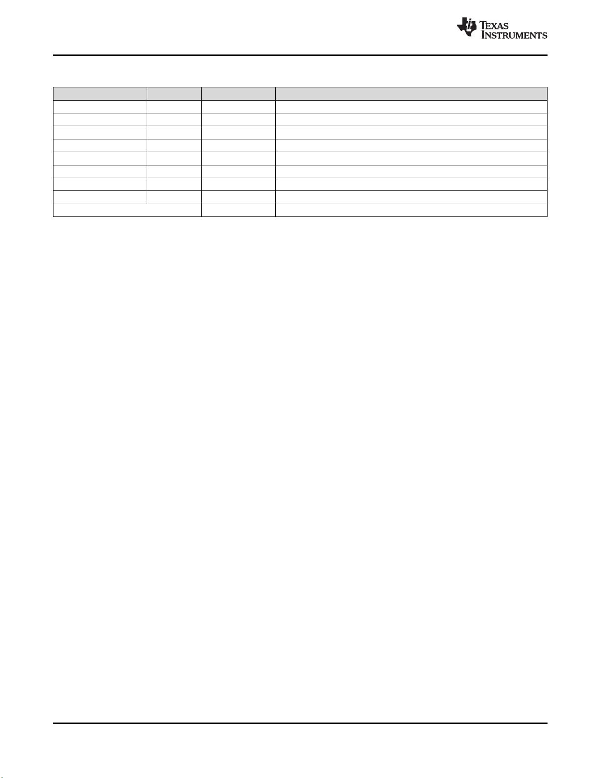
6. 安全与合规性:文档中提到的重要注意事项包括关于可用性、保修、安全关键应用使用、知识产权声明等,强调了生产数据的生产日期和修订历史。 这款CC2640R2F-Q1因其在汽车电子领域的高适应性和卓越性能,适用于各种汽车类应用,如舒适性、娱乐系统、远程信息处理和车辆网络通信等。它的设计旨在提供高效能、低功耗以及可靠的连接解决方案,是现代智能汽车技术中的关键组件之一。"
资源详情
资源推荐
8
CC2640R2F-Q1
ZHCSGW5A –JANUARY 2017–REVISED AUGUST 2017
www.ti.com.cn
Submit Documentation Feedback
Product Folder Links: CC2640R2F-Q1
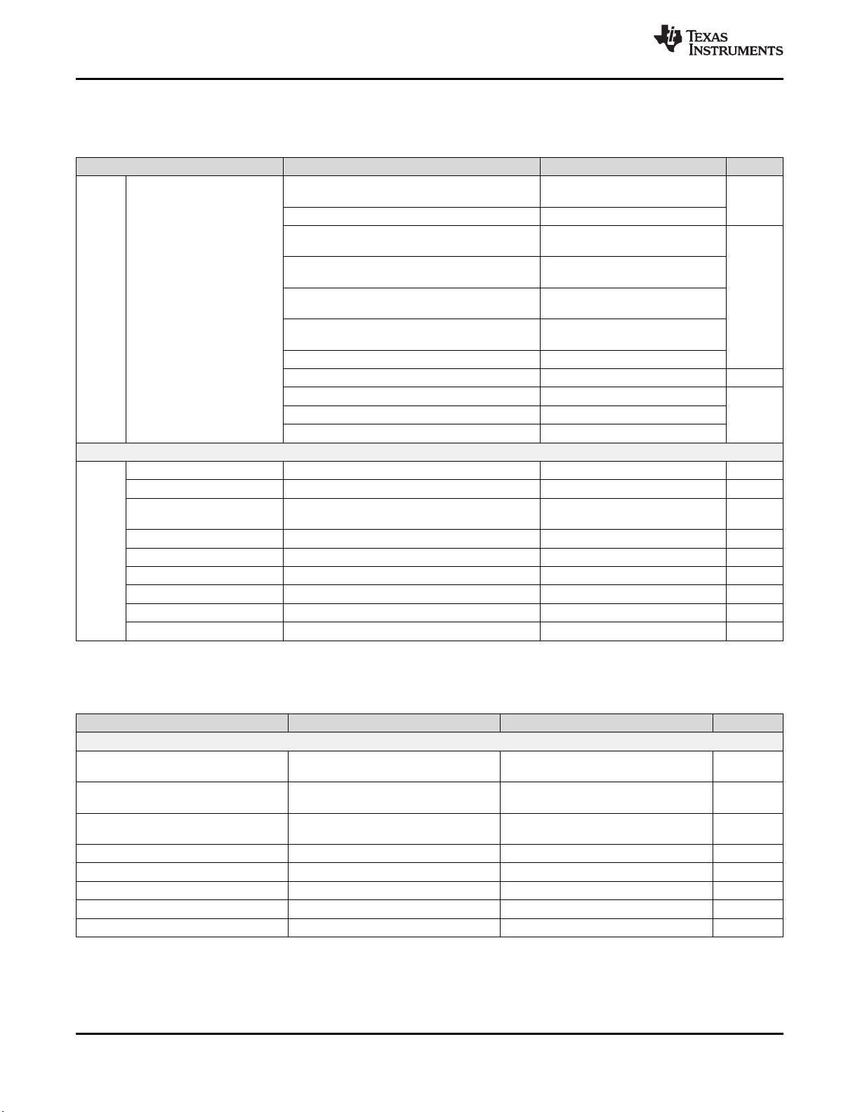
Terminal Configuration and Functions Copyright © 2017, Texas Instruments Incorporated
Table 4-1. Signal Descriptions – RGZ Package (continued)
NAME NO. TYPE DESCRIPTION
VDDS 44 Power 1.8-V to 3.8-V main chip supply
(1)
VDDS2 13 Power 1.8-V to 3.8-V DIO supply
(1)
VDDS3 22 Power 1.8-V to 3.8-V DIO supply
(1)
VDDS_DCDC 34 Power 1.8-V to 3.8-V DC/DC supply
X32K_Q1 3 Analog I/O 32-kHz crystal oscillator pin 1
X32K_Q2 4 Analog I/O 32-kHz crystal oscillator pin 2
X24M_N 46 Analog I/O 24-MHz crystal oscillator pin 1
X24M_P 47 Analog I/O 24-MHz crystal oscillator pin 2
EGP Power Ground – Exposed Ground Pad
4.3 Wettable Flanks
The automotive industry requires original equipment manufacturers (OEMs) to perform 100% automated
visual inspection (AVI) post-assembly to ensure that cars meet the current demands for safety and high
reliability. Standard quad-flat no-lead (VQFN) packages do not have solderable or exposed pins/terminals
that are easily viewed. It is therefore difficult to determine visually whether or not the package is
successfully soldered onto the printed circuit board (PCB). To resolve the issue of side-lead wetting of
leadless packaging for automotive and commercial component manufacturers, the wettable-flank process
was developed. The wettable flanks on the VQFN package provide a visual indicator of solderability and
thereby lower the inspection time and manufacturing costs.
The CC2640R2F-Q1 device is assembled using an automotive-grade VQFN package with wettable flanks.
9
CC2640R2F-Q1
www.ti.com.cn
ZHCSGW5A –JANUARY 2017–REVISED AUGUST 2017
Submit Documentation Feedback
Product Folder Links: CC2640R2F-Q1
SpecificationsCopyright © 2017, Texas Instruments Incorporated
(1) All voltage values are with respect to ground, unless otherwise noted.
(2) Stresses beyond those listed under Absolute Maximum Ratings may cause permanent damage to the device. These are stress ratings
only, and functional operation of the device at these or any other conditions beyond those indicated under Recommended Operating
Conditions is not implied. Exposure to absolute-maximum-rated conditions for extended periods may affect device reliability.
(3) VDDS2 and VDDS3 need to be at the same potential as VDDS.
(4) Including analog-capable DIO.
5 Specifications
5.1 Absolute Maximum Ratings
over operating free-air temperature range (unless otherwise noted)
(1)(2)
MIN MAX UNIT
Supply voltage, VDDS
(3)
VDDR supplied by internal DC/DC regulator or
internal GLDO. VDDS_DCDC connected to VDDS on
PCB.
–0.3 4.1 V
Voltage on any digital pin
(4)
–0.3 VDDS + 0.3, max 4.1 V
Voltage on crystal oscillator pins, X32K_Q1, X32K_Q2, X24M_N and X24M_P –0.3 VDDR + 0.3, max 2.25 V
Voltage on ADC input (V
in
)
Voltage scaling enabled –0.3 VDDS
VVoltage scaling disabled, internal reference –0.3 1.49
Voltage scaling disabled, VDDS as reference –0.3 VDDS / 2.9
Input RF level 5 dBm
T
stg
Storage temperature –40 150 °C
(1) AEC Q100-002 indicates HBM stressing is done in accordance with the ANSI/ESDA/JEDEC JS-001 specification.
(2) JEDEC document JEP155 states that 500-V HBM allows safe manufacturing with a standard ESD control process.
(3) JEDEC document JEP157 states that 250-V CDM allows safe manufacturing with a standard ESD control process.
5.2 ESD Ratings
VALUE UNIT
V
ESD
Electrostatic discharge
Human Body Model (HBM), per AEC Q100-002
(1)(2)
All pins ±2000
V
Charged Device Model (CDM), per AEC Q100-011
(3)
XOCS pins 46, 47 ±250
All other pins ±500
5.3 Recommended Operating Conditions
over operating free-air temperature range (unless otherwise noted)
MIN MAX UNIT
Ambient temperature –40 105 °C
Operating supply voltage,
VDDS
For operation in battery-powered and 3.3-V systems
(internal DC/DC can be used to minimize power consumption)
1.8 3.8 V
10
CC2640R2F-Q1
ZHCSGW5A –JANUARY 2017–REVISED AUGUST 2017
www.ti.com.cn
Submit Documentation Feedback
Product Folder Links: CC2640R2F-Q1
Specifications Copyright © 2017, Texas Instruments Incorporated
(1) I
peri
is not supported in Standby or Shutdown.
5.4 Power Consumption Summary
Measured on the TI CC2640Q1EM-7ID reference design with T
c
= 25°C, V
DDS
= 3.0 V with internal DC/DC converter, unless
otherwise noted.
PARAMETER TEST CONDITIONS MIN TYP MAX UNIT
I
core
Core current consumption
Reset. RESET_N pin asserted or VDDS below
power-on-reset (POR) threshold
100
nA
Shutdown. No clocks running, no retention 150
Standby. With RTC, CPU, RAM and (partial)
register retention. RCOSC_LF
1.3
µA
Standby. With RTC, CPU, RAM and (partial)
register retention. XOSC_LF
1.5
Standby. With Cache, RTC, CPU, RAM and
(partial) register retention. RCOSC_LF
3.4
Standby. With Cache, RTC, CPU, RAM and
(partial) register retention. XOSC_LF
3.6
Idle. Supply Systems and RAM powered. 650
Active. Core running CoreMark 1.45 mA + 31 µA/MHz
Radio RX 6.1
mARadio TX, 0-dBm output power 7.0
Radio TX, 5-dBm output power 9.3
Peripheral Current Consumption (Adds to core current I
core
for each peripheral unit activated)
(1)
I
peri
Peripheral power domain Delta current with domain enabled 20 µA
Serial power domain Delta current with domain enabled 13 µA
RF Core
Delta current with power domain enabled, clock
enabled, RF core idle
237 µA
µDMA Delta current with clock enabled, module idle 130 µA
Timers Delta current with clock enabled, module idle 113 µA
I
2
C Delta current with clock enabled, module idle 12 µA
I2S Delta current with clock enabled, module idle 36 µA
SSI Delta current with clock enabled, module idle 93 µA
UART Delta current with clock enabled, module idle 164 µA
(1) Each row is 2048 bits (or 256 bytes) wide.
(2) This number is dependent on Flash aging and will increase over time and erase cycles.
5.5 General Characteristics
T
c
= 25°C, V
DDS
= 3.0 V, unless otherwise noted.
PARAMETER TEST CONDITIONS MIN TYP MAX UNIT
FLASH MEMORY
Supported flash erase cycles before
failure
100 k Cycles
Maximum number of write operations
per row before erase
(1)
83
write
operations
Flash retention 105°C 11.4
Years at
105°C
Flash page/sector erase current Average delta current 12.6 mA
Flash page/sector size 4 KB
Flash write current Average delta current, 4 bytes at a time 8.15 mA
Flash page/sector erase time
(2)
8 ms
Flash write time
(2)
4 bytes at a time 8 µs
剩余45页未读,继续阅读
weixin_42981867
- 粉丝: 0
- 资源: 2
上传资源 快速赚钱
- 我的内容管理 展开
- 我的资源 快来上传第一个资源
- 我的收益 登录查看自己的收益
- 我的积分 登录查看自己的积分
- 我的C币 登录后查看C币余额
- 我的收藏
- 我的下载
- 下载帮助
最新资源
- 计算机人脸表情动画技术发展综述
- 关系数据库的关键字搜索技术综述:模型、架构与未来趋势
- 迭代自适应逆滤波在语音情感识别中的应用
- 概念知识树在旅游领域智能分析中的应用
- 构建is-a层次与OWL本体集成:理论与算法
- 基于语义元的相似度计算方法研究:改进与有效性验证
- 网格梯度多密度聚类算法:去噪与高效聚类
- 网格服务工作流动态调度算法PGSWA研究
- 突发事件连锁反应网络模型与应急预警分析
- BA网络上的病毒营销与网站推广仿真研究
- 离散HSMM故障预测模型:有效提升系统状态预测
- 煤矿安全评价:信息融合与可拓理论的应用
- 多维度Petri网工作流模型MD_WFN:统一建模与应用研究
- 面向过程追踪的知识安全描述方法
- 基于收益的软件过程资源调度优化策略
- 多核环境下基于数据流Java的Web服务器优化实现提升性能
资源上传下载、课程学习等过程中有任何疑问或建议,欢迎提出宝贵意见哦~我们会及时处理!
点击此处反馈
安全验证
文档复制为VIP权益,开通VIP直接复制
信息提交成功