没有合适的资源?快使用搜索试试~ 我知道了~
首页LTM4622:双路2.5A超薄开关电源μModule
LTM4622:双路2.5A超薄开关电源μModule
需积分: 50 10 下载量 20 浏览量
更新于2024-07-21
收藏 787KB PDF 举报
"LTM4622是一款双路2.5A超薄开关电源微模块(μModule)稳压器,适用于小封装高功率应用。" LTM4622是线性科技公司推出的一款高效能、紧凑型的双通道降压型直流-直流μModule稳压器,其封装尺寸仅为6.25mm x 6.25mm x 1.82mm,实现了在小体积下提供大功率输出的能力。该器件在输入电压范围为3.6V至20V的情况下,可以为两个通道分别提供最高2.5A的连续电流,峰值电流可达3A,并且可以通过一个外部电阻设定输出电压,范围在0.6V到5.5V之间。 LTM4622的特性之一是可选择的Burst Mode(间歇模式)操作,这种模式在轻负载时降低开关频率以减少功耗,同时支持输出电压追踪功能,便于电源轨的顺序控制。此外,其高开关频率结合电流模式控制技术,确保了对线路和负载变化的快速响应,实现了良好的动态性能,而不会牺牲系统稳定性。 该稳压器还集成了多种保护功能,包括输入过电压保护、输出过电流保护和过温保护,以确保在各种工作条件下的系统安全。LTM4622符合RoHS标准,采用无铅表面处理。 在具体应用中,LTM4622通常需要配合少量的陶瓷输入和输出电容器使用,以完成完整的电源解决方案。例如,1.5V和1V的双输出配置,可以满足许多高性能数字和模拟电路的供电需求,特别是在空间有限但功率需求较高的场合,如嵌入式系统、通信设备和工业控制等领域。 LTM4622凭借其小巧的封装、高效的性能和全面的保护机制,成为现代电子设计中实现双路低电压、高电流电源供应的理想选择。其灵活性和易用性使得它能够适应多种多样的应用场景,为工程师提供了强大的电源管理工具。
资源详情
资源推荐
LTM4622
5
4622f
For more information www.linear.com/LTM4622
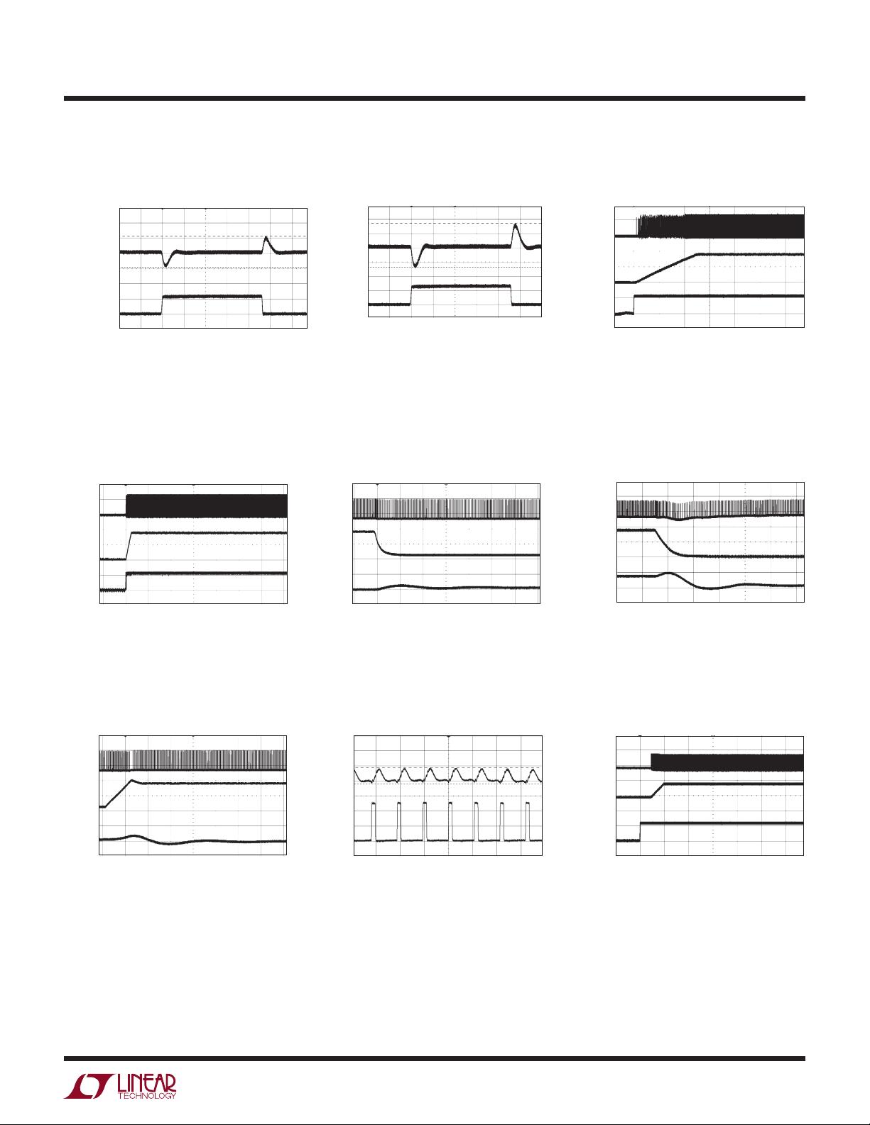
3.3V Output Transient Response
5V Output Transient Response
Start-Up with No Load Current
Applied
Start-Up with 2.5A Load Current
Applied
Recover from Short-Circuit with
No Load Current Applied
Short-Circuit with No Load
Current Applied
Short-Circuit with 2.5A Load
Current Applied
Steady-State Output Voltage
Ripple
Start-Up into Pre-Biased Output
TYPICAL PERFORMANCE CHARACTERISTICS
V
OUT
100mV/DIV
AC-COUPLED
LOAD STEP
1A/DIV
V
IN
= 12V
V
OUT
= 3.3V
F
S
= 2MHz
OUTPUT CAPACITOR = 1 × 47µF CERAMIC
LOAD STEP = 1.25A TO 2.5A
20µs/DIV
4622 G09
V
OUT
100mV/DIV
AC-COUPLED
LOAD STEP
1A/DIV
V
IN
= 12V
V
OUT
= 5V
F
S
= 2.5MHz
OUTPUT CAPACITOR = 1 × 47µF CERAMIC
LOAD STEP = 1.25A TO 2.5A
20µs/DIV
4622 G10
SW
10V/DIV
V
OUT
1V/DIV
RUN
10V/DIV
V
IN
= 12V
V
OUT
= 1.8V
F
S
= 1MHz
INPUT CAPACITOR = 1 × 22µF
OUTPUT CAPACITOR = 1 × 22µF + 1 × 47µF CERAMIC
SOFT-START CAP = 0.1µF
20ms/DIV
4622 G11
SW
10V/DIV
V
OUT
1V/DIV
RUN
10V/DIV
V
IN
= 12V
V
OUT
= 1.8V
F
S
= 1MHz
INPUT CAPACITOR = 1 × 22µF
OUTPUT CAPACITOR = 1 × 22µF + 1 × 47µF CERAMIC
SOFT-START CAP = 0.1µF
200ms/DIV
4622 G12
SW
10V/DIV
V
OUT
1V/DIV
I
IN
2A/DIV
V
IN
= 12V
V
OUT
= 1.8V
F
S
= 1MHz
INPUT CAPACITOR = 1 × 22µF
OUTPUT CAPACITOR = 1 × 22µF + 1 × 47µF CERAMIC
20µs/DIV
4622 G13
SW
10V/DIV
V
OUT
1V/DIV
I
IN
2A/DIV
V
IN
= 12V
V
OUT
= 1.8V
F
S
= 1MHz
INPUT CAPACITOR = 1 × 22µF
OUTPUT CAPACITOR = 1 × 22µF + 1 × 47µF CERAMIC
20µs/DIV
4622 G15
V
OUT
10mV/DIV
AC-COUPLED
SW
5V/DIV
V
IN
= 12V
V
OUT
= 1.8V
F
S
= 1MHz
INPUT CAPACITOR = 1 × 22µF
OUTPUT CAPACITOR = 1 × 22µF + 1 × 47µF CERAMIC
1µs/DIV
4622 G16
SW
10V/DIV
V
OUT
1V/DIV
I
IN
500mA/DIV
V
IN
= 12V
V
OUT
= 1.8V
F
S
= 1MHz
INPUT CAPACITOR = 1 × 22µF
OUTPUT CAPACITOR = 1 × 22µF + 1 × 47µF CERAMIC
20µs/DIV
4622 G14
SW
10V/DIV
V
OUT
1V/DIV
RUN
10V/DIV
V
IN
= 12V
V
OUT
= 1.8V
F
S
= 1MHz
INPUT CAPACITOR = 1 × 22µF
OUTPUT CAPACITOR = 1 × 22µF + 1 × 47µF CERAMIC
50ms/DIV
4622 G17
LTM4622
6
4622f
For more information www.linear.com/LTM4622
PIN FUNCTIONS
V
IN
(A2, B3, D3, E2): Power Input Pins. Apply input voltage
between these pins and GND pins. Recommend placing
input decoupling capacitance directly between V
IN
pins
and GND pins.
GND (C1 to C2, B5, D5): Power Ground Pins for Both
Input and Output Returns.
INTV
CC
(C3): Internal 3.3V Regulator Output. The internal
power drivers and control circuits are powered from this
voltage
. This pin is internally decoupled to GND with a
2.2µF low ESR ceramic capacitor. No additional external
decoupling capacitor needed.
SYNC/MODE (C5): Mode Select and External Synchroni-
zation Input. Tie this pin to ground to force continuous
synchronous operation at all output loads. Floating this
pin or tying it to INTV
CC
enables high efficiency Burst
Mode operation at light loads. Drive this pin with
a clock
to synchronize the LTM4622 switching frequency. An
internal phase-locked loop will force the bottom power
NMOS’s turn on signal to be synchronized with the rising
edge of the clock signal. When this pin is driven with a
clock, forced continuous mode is automatically selected.
V
OUT1
(D1, E1), V
OUT2
(A1, B1): Power Output Pins
of Each Switching Mode Regulator. Apply output
load
between these pins and GND pins. Recommend placing
output decoupling capacitance directly between these
pins and GND pins.
FREQ (C4): Frequency is set internally to 1MHz. An ex-
ternal resistor can be placed from this pin to SGND to
increase frequency, or from this pin to INTV
CC
to reduce
frequency. See the Applications Information section for
frequency adjustment.
RUN1 (D2), RUN2 (B2): Run Control Input
of Each Switch-
ing Mode Regulator Channel. Enables chip operation by
tying RUN above 1.22V. Tying this pin below 1V shuts
down the specific regulator channel. Do not float this pin.
PGOOD1 (D4), PGOOD2 (B4): Output Power Good with
Open-Drain Logic of Each Switching Mode Regulator
Channel. PGOOD is pulled to ground when the voltage
on the FB pin is not within ±8% (typical) of the
internal
0.6V reference.
TRACK/SS1 (E3), TRACK/SS2 (A3): Output Tracking
and Soft-Start Pin of Each Switching Mode Regulator
Channel. It allows the user to control the rise time of the
output voltage. Putting a voltage below 0.6V on this pin
bypasses the internal reference input to the error ampli-
fier, instead it servos the FB pin to the TRACK voltage.
Above 0.6V, the tracking
function stops and the internal
reference resumes control of the error amplifier. There’s
an internal 1.4µA pull-up current from INTV
CC
on this pin,
so putting a capacitor here provides soft-start function.
A default internal soft-start ramp forces a minimum soft-
start time of 400ms.
FB1 (E4), FB2 (A4): The Negative Input of the Error Ampli-
fier for Each Switching Mode Regulator Channel.
Inter-
nally, this pin is connected to V
OUT
with a 60.4k precision
resistor. Different output voltages can be programmed
with an additional resistor between FB and GND pins. In
PolyPhase
®
operation, tying the FB pins together allows
for parallel operation. See the Applications Information
section for details.
COMP1 (E5), COMP2 (A5): Current Control Threshold
and Error Amplifier Compensation Point of Each Switch-
ing Mode Regulator Channel
. The current comparator’s
trip threshold is linearly proportional to this voltage,
whose normal range is from 0.3V to 1.8V. Tie the COMP
pins together for parallel operation. The device is internal
compensated. Do not drive this pin.
PACKAGE ROW AND COLUMN LABELING MAY VARY
AMONG µModule PRODUCTS. REVIEW EACH PACKAGE
LAYOUT CAREFULLY.
剩余25页未读,继续阅读
baidu_30650639
- 粉丝: 0
- 资源: 1
上传资源 快速赚钱
- 我的内容管理 展开
- 我的资源 快来上传第一个资源
- 我的收益 登录查看自己的收益
- 我的积分 登录查看自己的积分
- 我的C币 登录后查看C币余额
- 我的收藏
- 我的下载
- 下载帮助
最新资源
- C++多态实现机制详解:虚函数与早期绑定
- Java多线程与异常处理详解
- 校园导游系统:无向图实现最短路径探索
- SQL2005彻底删除指南:避免重装失败
- GTD时间管理法:提升效率与组织生活的关键
- Python进制转换全攻略:从10进制到16进制
- 商丘物流业区位优势探究:发展战略与机遇
- C语言实训:简单计算器程序设计
- Oracle SQL命令大全:用户管理、权限操作与查询
- Struts2配置详解与示例
- C#编程规范与最佳实践
- C语言面试常见问题解析
- 超声波测距技术详解:电路与程序设计
- 反激开关电源设计:UC3844与TL431优化稳压
- Cisco路由器配置全攻略
- SQLServer 2005 CTE递归教程:创建员工层级结构
资源上传下载、课程学习等过程中有任何疑问或建议,欢迎提出宝贵意见哦~我们会及时处理!
点击此处反馈
安全验证
文档复制为VIP权益,开通VIP直接复制
信息提交成功