TI DS160UP822:高性能8通道PCI转接线性驱动器
TI-DS160UP822是一款高性能的PCI转接驱动器,专为满足现代数据中心和高性能计算应用的需求而设计。该产品的主要特点包括:
1. **高速接口支持**:DS160UP822支持UPI 2.0标准,能够提供高达16 Gbps的数据传输速率,适用于对带宽需求极高的接口,如DisplayPort、SAS、SATA和XFI。
2. **多协议兼容性**:作为线性重新驱动器,DS160UP822具有协议无关特性,能够在多种高速数据接口间无缝转换,灵活性极高。
3. **交叉点多路复用**:提供四个2x2交叉点功能,允许用户根据需要配置不同的数据传输宽度,如x4、x8、x16或x24。
4. **高增益与低时延**:内置的CTLE(电流模式逻辑电平转换器)在8 GHz频率下能提供高达18 dB的增益,同时保持极低的延迟,仅为90 ps,有利于减少数据传输中的信号失真。
5. **低噪声性能**:采用先进的技术,添加随机噪声极低,只有70 fs的Jitter,即使在PRBS(伪随机二进制序列)数据条件下,也能确保数据传输的稳定性。
6. **电源效率**:DS160UP822工作在单个3.3 V电压下,每个通道的平均功耗低至107 mW,节省能源的同时降低了系统的热负荷。
7. **无散热器需求**:由于其高效的设计,无需额外的散热设备,简化了系统集成。
8. **编程灵活性**:通过Pin-strap、SMBus/I2C或EEPROM进行配置,方便灵活地调整和管理设备特性。
9. **无缝链路训练**:支持无缝的链路训练过程,确保连接稳定可靠。
10. **宽温度范围**:设计适应工业环境,可在-40°C至85°C的极端温度范围内稳定运行,增加了其应用的广泛性。
11. **紧凑封装**:采用紧凑的5.5mm × 10mm、64-pin WQFN封装,占用空间小,适合于小型化和模块化设计。
这款驱动器主要应用于服务器市场,包括机架服务器、微服务器和塔式服务器,以及需要硬件加速的高性能计算领域。它的设计和特性使得它成为构建高速、低延迟、能耗高效的系统架构的理想选择。
6 Specifications
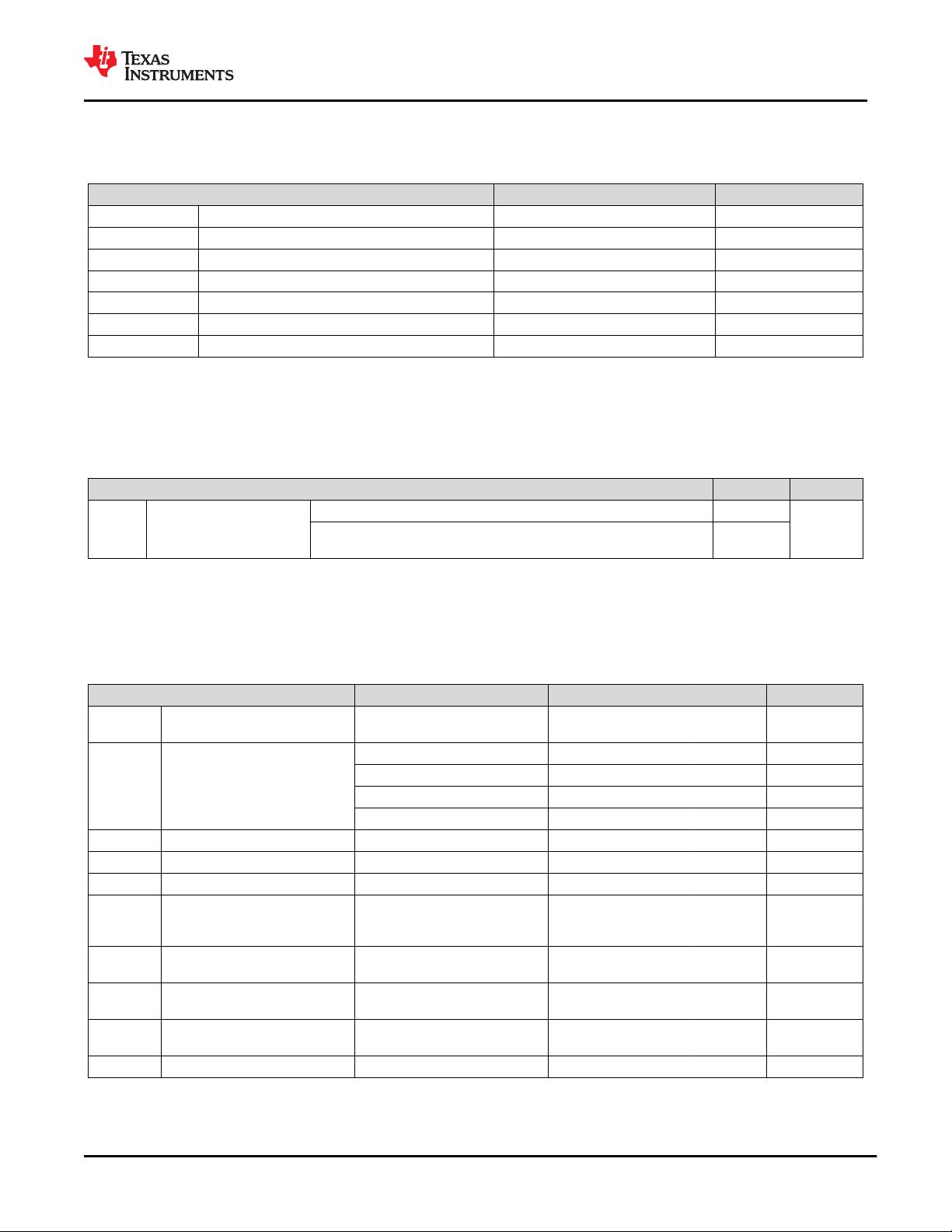
6.1 Absolute Maximum Ratings
over operating free-air temperature range (unless otherwise noted)
(1)
MIN MAX UNIT
VCC
ABSMAX
Supply voltage (VCC) –0.5 4.0 V
VIO
CMOS,ABSMAX
3.3 V LVCMOS and open drain I/O voltage –0.5 4.0 V
VIO
4LVL,ABSMAX
4-level input I/O voltage –0.5 2.75 V
VIO
HS-RX,ABSMAX
High-speed I/O voltage (RXnP, RXnN) –0.5 3.2 V
VIO
HS-TX,ABSMAX
High-speed I/O voltage (TXnP, TXnN) –0.5 2.75 V
T
J,ABSMAX
Junction temperature 150 °C
T
stg
Storage temperature range –65 150 °C
(1) Stresses beyond those listed under Absolute Maximum Ratings may cause permanent damage to the device. These are stress ratings
only, which do not imply functional operation of the device at these or any other conditions beyond those indicated under
Recommended Operating Conditions. Exposure to absolute-maximum-rated conditions for extended periods may affect device
reliability.
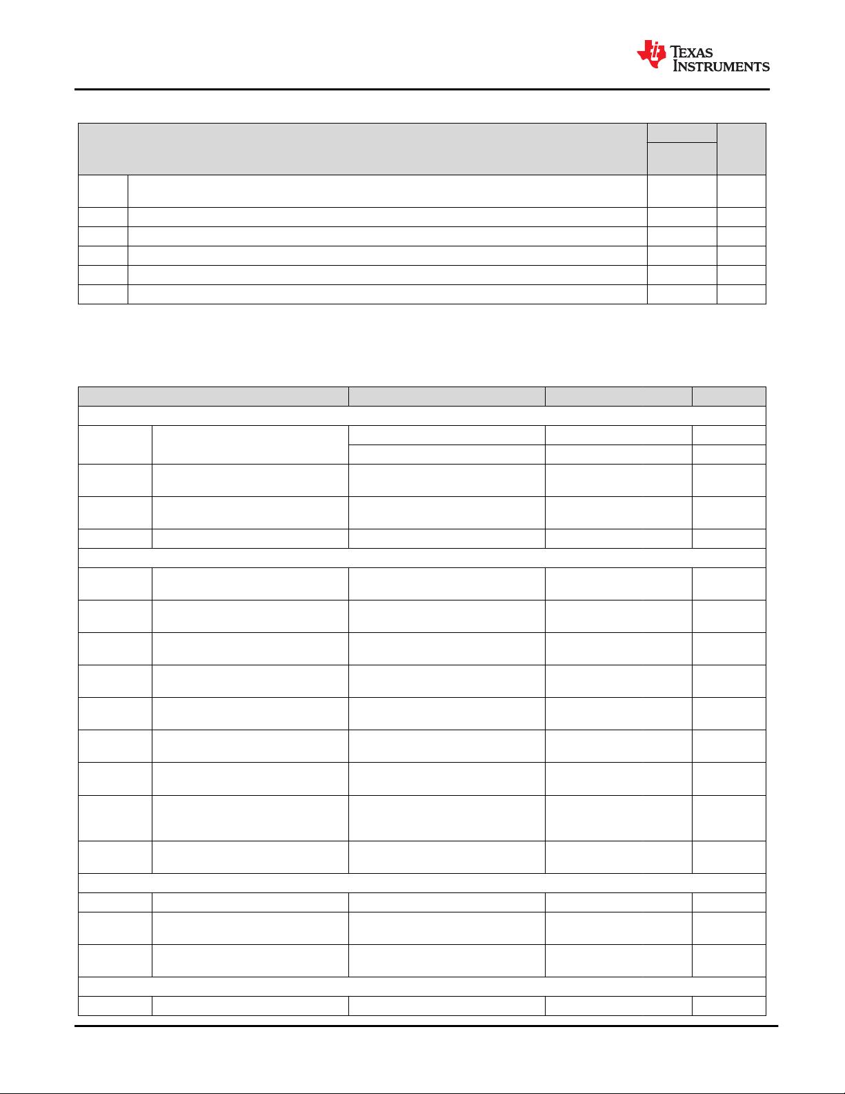
6.2 ESD Ratings
VALUE UNIT
V
(ESD)
Electrostatic discharge
Human body model (HBM), per ANSI/ESDA/JEDEC JS-001
(1)
±3000
V
Charged device model (CDM), per JEDEC specification JESD22-
C101
(2)
±500
(1) JEDEC document JEP155 states that 500-V HBM allows safe manufacturing with a standard ESD control process. Pins listed as ±3 kV
may actually have higher performance.
(2) JEDEC document JEP157 states that 250-V CDM allows safe manufacturing with a standard ESD control process.
6.3 Recommended Operating Conditions
over operating free-air temperature range (unless otherwise noted)
MIN NOM MAX UNIT
VCC Supply voltage, VCC to GND
DC plus AC power should not
exceed these limits
3.0 3.3 3.6 V
N
VCC
Supply noise tolerance
1
DC to <50 Hz, sinusoidal 250 mVpp
50 Hz to 500 kHz, sinusoidal 100 mVpp
500 kHz to 2.5 MHz, sinusoidal 33 mVpp
>2.5 MHz, sinusoidal 10 mVpp
T
RampVCC
VCC supply ramp time From 0 V to 3.0 V 0.150 100 ms
T
J
Operating junction temperature –40 115 °C
T
A
Operating ambient temperature –40 85 °C
PW
LVCMOS
Minimum pulse width required for
the device to detect a valid signal
on LVCMOS inputs
PD1/0, and READ_EN_N 200 uS
VCC
SMBUS
SMBus/I
2
C SDA and SCL open
drain termination voltage
Supply voltage for open drain
pull-up resistor
3.6 V
F
SMBus
SMBus/I
2
C clock (SCL) frequency
in SMBus slave mode
10 400 kHz
VID
LAUNCH
Source differential launch
amplitude
800 1200 mVpp
DR Data rate 1 16 Gbps
www.ti.com
DS160UP822
SNLS680 – DECEMBER 2020
Copyright © 2020 Texas Instruments Incorporated
Submit Document Feedback
7
Product Folder Links: DS160UP822
剩余35页未读,继续阅读
点击了解资源详情
点击了解资源详情
点击了解资源详情
2023-02-09 上传
2023-02-09 上传
2023-02-09 上传
2023-02-09 上传
2023-02-09 上传

不觉明了
- 粉丝: 7423
- 资源: 5764
 我的内容管理
展开
我的内容管理
展开


最新资源
- 实战部署UC平台(OCS=VOIP GW=Exchange2007).pdf
- thinking in java
- 嵌入式Linux Framebuffer 驱动开发.pdf
- grails入门指南
- Apress.Pro.OGRE.3D.Programming.pdf
- Linux设备驱动开发详解讲座.pdf
- GoF+23种设计模式
- Wrox.Python.Create.Modify.Reuse.Jul.2008
- sd卡spi模式翻译资料
- 最新计算机考研专业课程大纲
- oracleproc编程
- Google-Guice-Agile-Lightweight-Dependency-Injection-Framework-Firstpress
- oracle工具TOAD快速入门
- Unix 操作命令大全
- ARM映象文件及执行机理
- rhce教材RH033 - Red Hat Linux Essentials
