
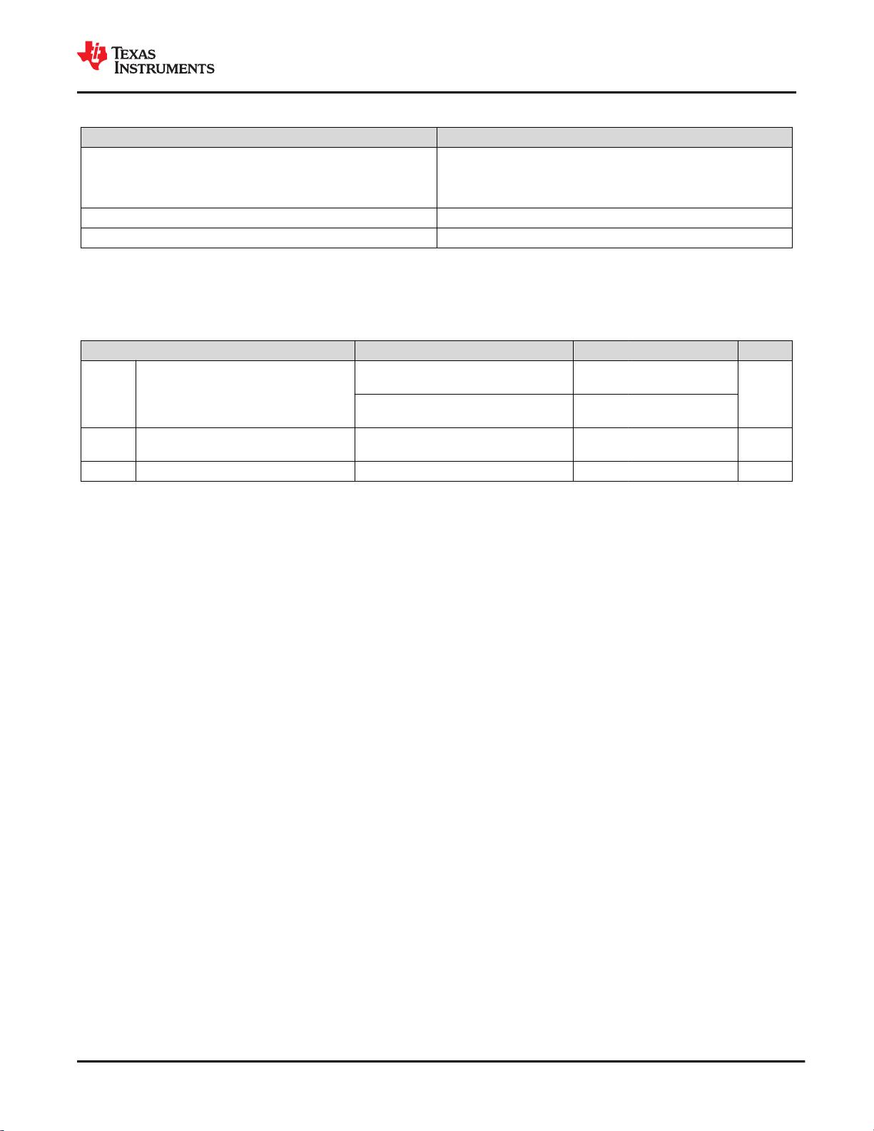
6.7 Safety-Related Certifications
VDE UL
Certified according to DIN VDE V 0884-11 (VDE V 0884-11):
2017-01,
DIN EN 60950-1 (VDE 0805 Teil 1): 2014-08, and
DIN EN 60065 (VDE 0860): 2005-11
Recognized under 1577 component recognition and
CSA component acceptance NO 5 programs
Reinforced insulation
Single protection
Certificate number: 40040142 File number: E181974
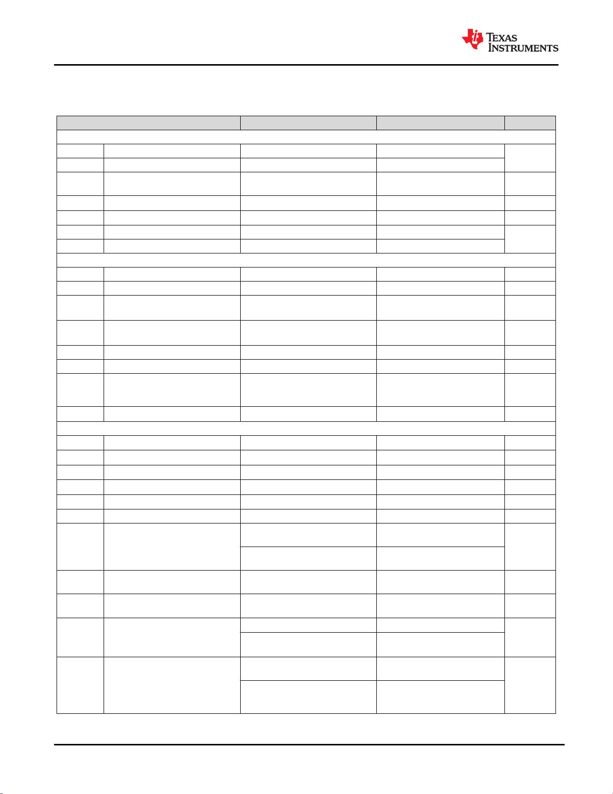
6.8 Safety Limiting Values
Safety limiting
(1)
intends to minimize potential damage to the isolation barrier upon failure of input or output circuitry. A failure
of the I/O can allow low resistance to ground or the supply and, without current limiting, dissipate sufficient power to over-
heat the die and damage the isolation barrier potentially leading to secondary system failures.
PARAMETER TEST CONDITIONS MIN TYP MAX UNIT
I
S
Safety input, output, or supply current
R
θJA
= 73.5°C/W, VDD = 5.5 V,
T
J
= 150°C, T
A
= 25°C
309
mA
R
θJA
= 73.5°C/W, VDD = 3.6 V,
T
J
= 150°C, T
A
= 25°C
472
P
S
Safety input, output, or total power
R
θJA
= 73.5°C/W,
T
J
= 150°C, T
A
= 25°C
1700 mW
T
S
Maximum safety temperature 150 °C
(1) The maximum safety temperature, T
S
, has the same value as the maximum junction temperature, T
J
, specified for the device. The I
S
and P
S
parameters represent the safety current and safety power, respectively. Do not exceed the maximum limits of I
S
and P
S
. These
limits vary with the ambient temperature, T
A
.
The junction-to-air thermal resistance, R
θJA
, in the Thermal Information table is that of a device installed on a high-K test board for
leaded surface-mount packages. Use these equations to calculate the value for each parameter:
T
J
= T
A
+ R
θJA
× P, where P is the power dissipated in the device.
T
J(max)
= T
S
= T
A
+ R
θJA
× P
S
, where T
J(max)
is the maximum junction temperature.
P
S
= I
S
× VDD
max
, where VDD
max
is the maximum low-side voltage.
www.ti.com.cn
AMC3330-Q1
ZHCSKS7A – JUNE 2020 – REVISED OCTOBER 2020
Copyright © 2021 Texas Instruments Incorporated
Submit Document Feedback
7
Product Folder Links: AMC3330-Q1
剩余36页未读,继续阅读


