
88
87
86
85
84
83
82
81
80
79
78
77
76
75
74
73
72
71
70
69
68
67
66
65
64
63
62
61
60
59
58
57
56
55
54
53
52
51
50
49
48
47
46
45
133
134
135
136
137
138
139
140
141
142
143
144
145
146
147
148
149
150
151
152
153
154
155
156
157
158
159
160
161
162
163
164
165
166
167
168
169
170
171
172
173
174
175
176
1
2
3
4
5
6
7
8
9
10
11
12
13
14
15
16
17
18
19
20
21
22
23
24
25
26
27
28
29
30
31
32
33
34
35
36
37
38
39
40
41
42
43
44
132
131
130
129
128
127
126
125
124
123
122
121
120
119
118
117
116
115
114
113
112
111
110
109
108
107
106
105
104
103
102
101
100
99
98
97
96
95
94
93
92
91
90
89
V
DD
V
DD
V
DDA
V
REFHIB
V
REFLOB
V
REFLOD
V
REFHID
V
SSA
GPIO40
GPIO39
GPIO38
GPIO37
TCK
TMS
TDO
TDI
GPIO35
GPIO34
GPIO33
GPIO32
GPIO31
GPIO29
GPIO28
GPIO30
ADCIND4
ADCIND3
ADCIND2
ADCIND1
ADCIND0
ADCINB3
ADCINB2
ADCINB1
ADCINB0
ADCIN15
FLT1
FLT2
TRST
GPIO36
V
DDIO
V
DDIO
V
DDIO
V
DDIO
V
DDIO
V
DD3VFL
GPIO67
GPIO133
GPIO45
GPIO44
GPIO66
GPIO65
GPIO64
GPIO63
GPIO62
GPIO61
GPIO60
GPIO59
GPIO58
GPIO57
GPIO56
GPIO55
GPIO54
GPIO53
GPIO52
GPIO51
GPIO50
GPIO49
GPIO48
GPIO41
ERRORSTS
VREGENZ
X1
X2
XRS
GPIO43
GPIO42
GPIO47
GPIO46
V
SSOSC
V
DD
V
DD
V
DDIO
V
DDOSC
V
DDOSC
V
DDIO
V
DDIO
V
DDIO
V
DDIO
V
DDIO
GPIO10
GPIO11
GPIO12
GPIO13
GPIO14
GPIO15
GPIO16
GPIO17
GPIO18
GPIO19
GPIO20
GPIO8
GPIO9
GPIO22
GPIO23
GPIO24
GPIO25
GPIO26
GPIO27
ADCINC4
ADCINC3
ADCINC2
ADCINA5
ADCINA4
ADCINA3
ADCINA2
ADCINA1
ADCINA0
ADCIN14
GPIO21
V
SSA
V
DDA
V
REFHIC
V
REFLOC
V
REFLOA
V
REFHIA
V
DD
GPIO99
V
DD
V
DDIO
V
DDIO
V
DDIO
V
DDIO
V
DDIO
GPIO68
GPIO69
GPIO70
GPIO71
GPIO72
GPIO73
GPIO74
GPIO75
GPIO76
GPIO77
GPIO78
GPIO79
GPIO80
GPIO81
GPIO82
GPIO83
GPIO0
GPIO1
GPIO2
GPIO3
GPIO4
GPIO5
GPIO6
GPIO7
GPIO88
GPIO89
GPIO90
GPIO91
GPIO92
GPIO93
GPIO94
GPIO84
GPIO85
GPIO86
GPIO87
V
DD
V
DD
V
DD
V
DDIO
V
DDIO
V
DDIO
V
DDIO
V
DDIO
V
DD
16
TMS320F28379D
,
TMS320F28378D
,
TMS320F28377D
TMS320F28376D, TMS320F28375D, TMS320F28374D
SPRS880M –DECEMBER 2013–REVISED JUNE 2020
www.ti.com
Submit Documentation Feedback
Product Folder Links: TMS320F28379D TMS320F28378D TMS320F28377D TMS320F28376D TMS320F28375D
TMS320F28374D
Terminal Configuration and Functions Copyright © 2013–2020, Texas Instruments Incorporated
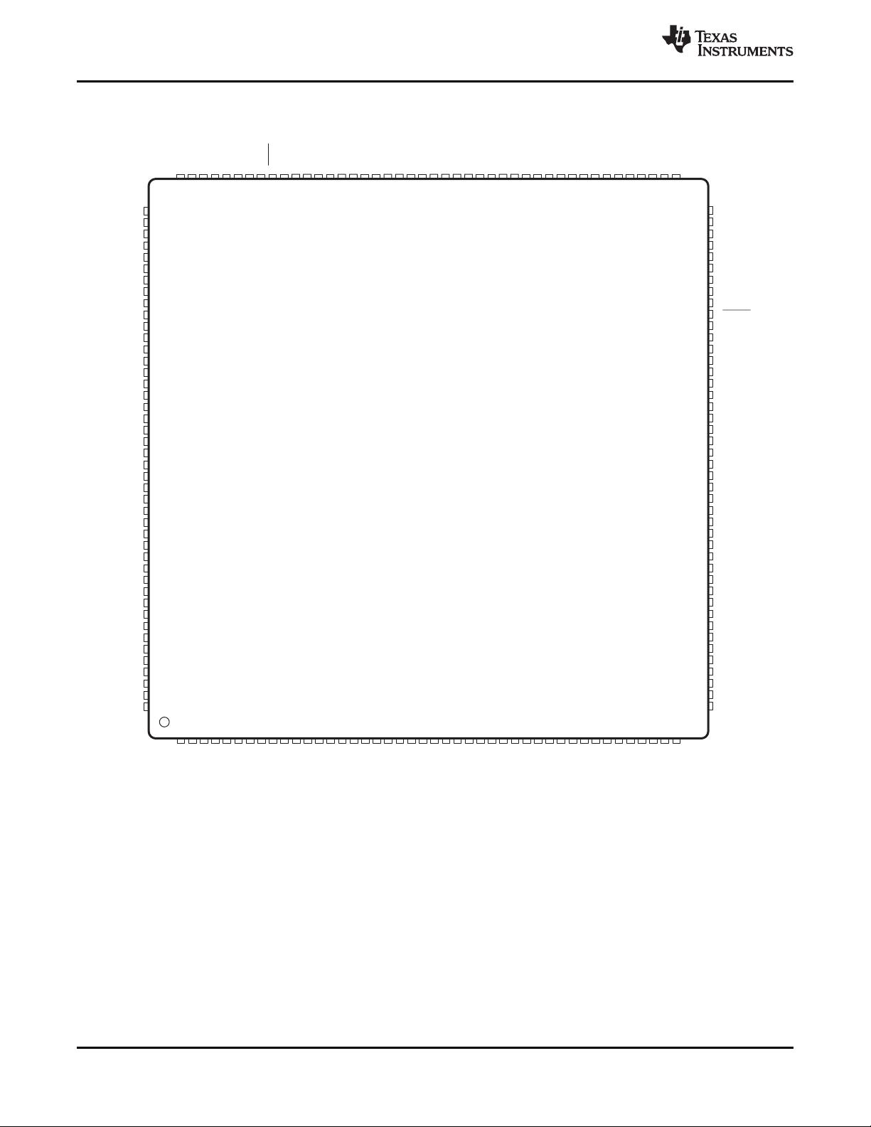
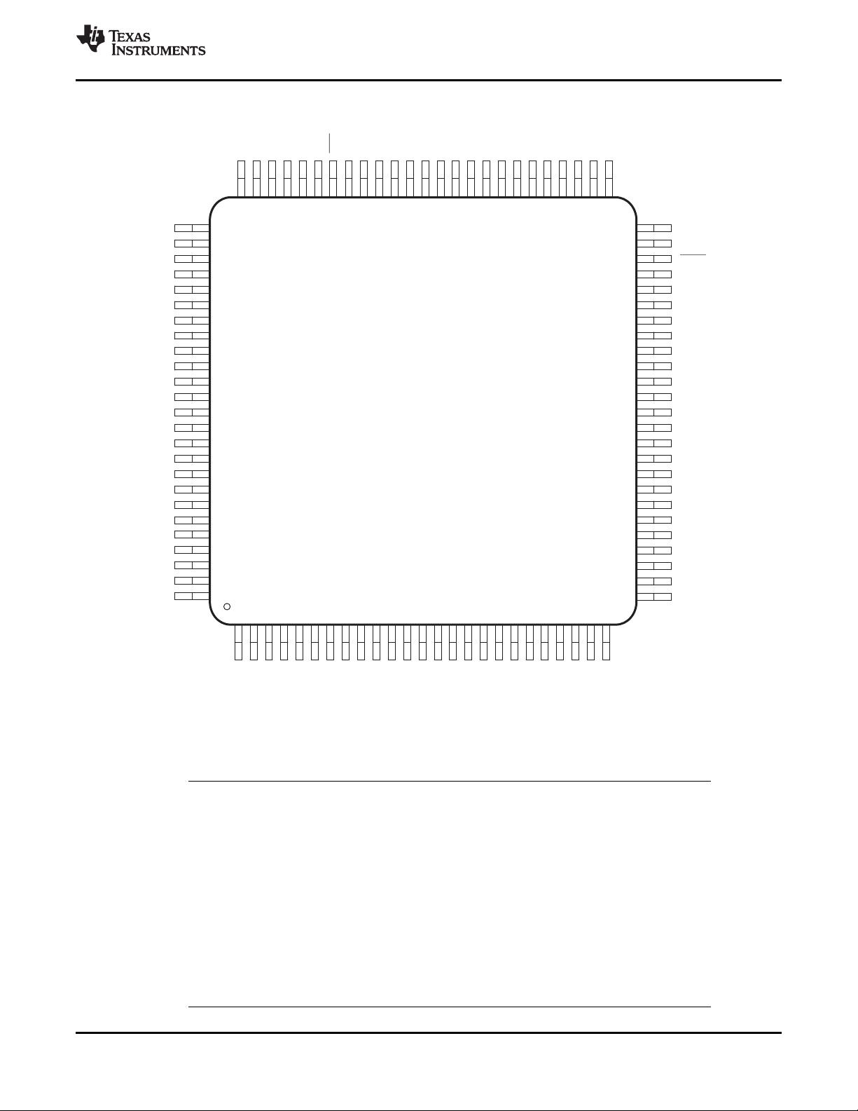
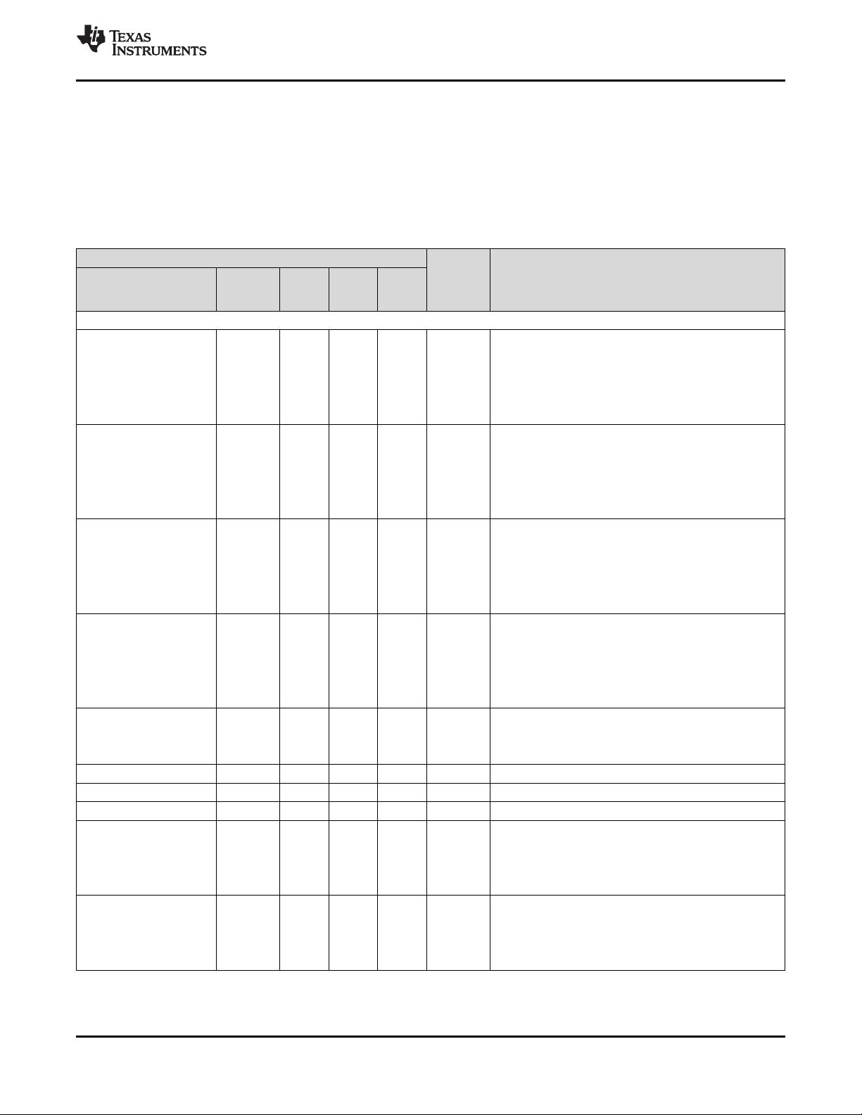
A. Only the GPIO function is shown on GPIO pins. See Table 4-1 for the complete, muxed signal name.
Figure 4-5. 176-Pin PTP PowerPAD Thermally Enhanced Low-Profile Quad Flatpack (Top View)


剩余228页未读,继续阅读

小娟娟zj
- 粉丝: 3
- 资源: 23
 我的内容管理
展开
我的内容管理
展开


最新资源
- C++多态实现机制详解:虚函数与早期绑定
- Java多线程与异常处理详解
- 校园导游系统:无向图实现最短路径探索
- SQL2005彻底删除指南:避免重装失败
- GTD时间管理法:提升效率与组织生活的关键
- Python进制转换全攻略:从10进制到16进制
- 商丘物流业区位优势探究:发展战略与机遇
- C语言实训:简单计算器程序设计
- Oracle SQL命令大全:用户管理、权限操作与查询
- Struts2配置详解与示例
- C#编程规范与最佳实践
- C语言面试常见问题解析
- 超声波测距技术详解:电路与程序设计
- 反激开关电源设计:UC3844与TL431优化稳压
- Cisco路由器配置全攻略
- SQLServer 2005 CTE递归教程:创建员工层级结构
资源上传下载、课程学习等过程中有任何疑问或建议,欢迎提出宝贵意见哦~我们会及时处理!
点击此处反馈


