6
LMK00334-Q1
ZHCSI14 –APRIL 2018
www.ti.com.cn
Copyright © 2018, Texas Instruments Incorporated
Electrical Characteristics (continued)
Unless otherwise specified: V
CC
= 3.3 V ± 5%, V
CCO
= 3.3 V ± 5%, 2.5 V ± 5%, –40°C ≤ T
A
≤ 105°C, CLKin driven
differentially, input slew rate ≥ 3 V/ns. Typical values represent the most likely parametric norms at V
CC
= 3.3 V, V
CCO
= 3.3 V,
T
A
= 25°C, and at the Recommended Operation Conditions at the time of product characterization; because of this, typical
values are not ensured.
(1)
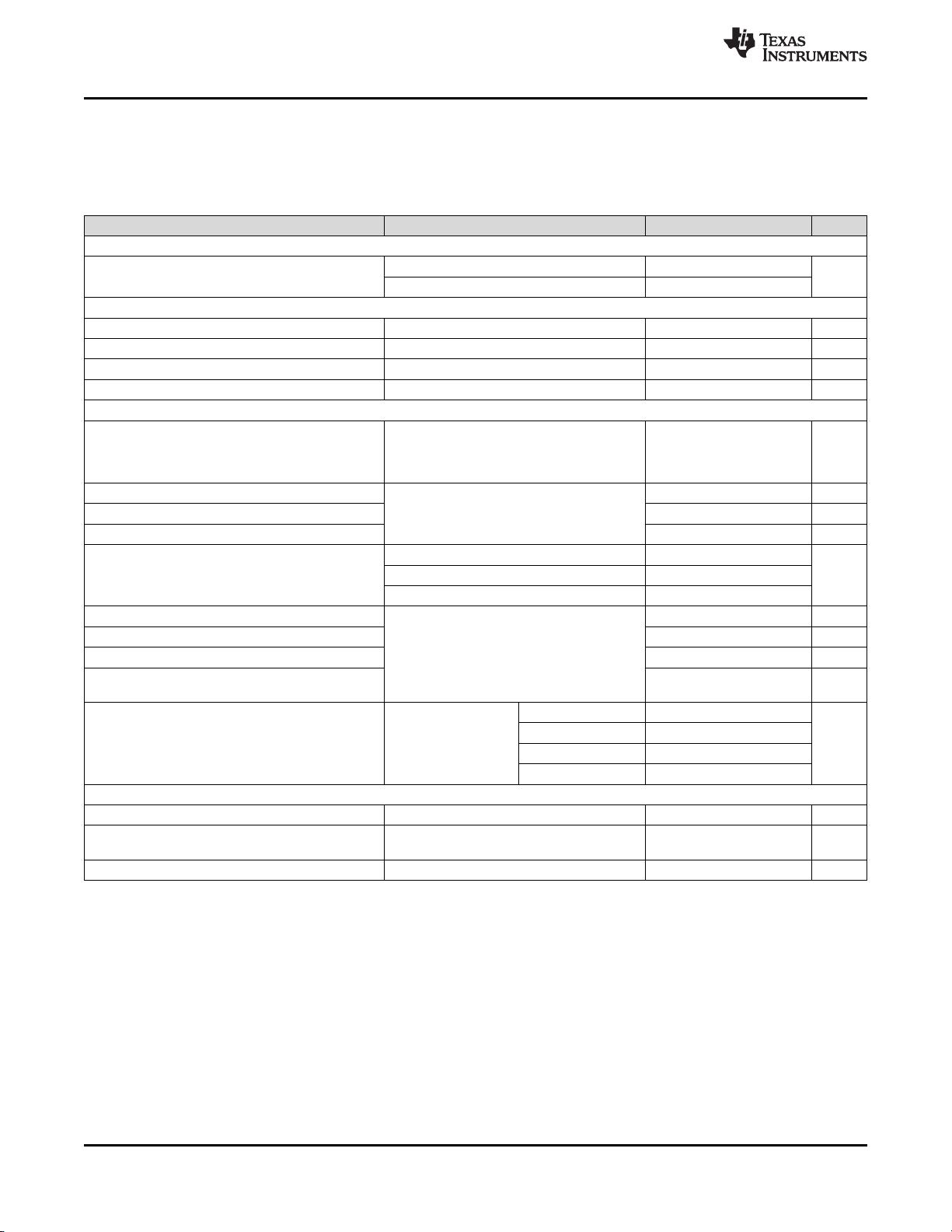
PARAMETER TEST CONDITIONS MIN TYP MAX UNIT
(3) Power supply ripple rejection, or PSRR, is defined as the single-sideband phase spur level (in dBc) modulated onto the clock output
when a single-tone sinusoidal signal (ripple) is injected onto the V
CCO
supply. Assuming no amplitude modulation effects and small
index modulation, the peak-to-peak deterministic jitter (DJ) can be calculated using the measured single-sideband phase spur level
(PSRR) as follows: DJ (ps pk-pk) = [ (2 × 10
(PSRR / 20)
) / (π × f
CLK
) ] × 1E12
(4) Specification is ensured by characterization and is not tested in production.
(5) See Differential Voltage Measurement Terminology for definition of V
ID
and V
OD
voltages.
(6) The ESR requirements stated must be met to ensure that the oscillator circuitry has no startup issues. However, lower ESR values for
the crystal may be necessary to stay below the maximum power dissipation (drive level) specification of the crystal. Refer to Crystal
Interface for crystal drive level considerations.
POWER SUPPLY RIPPLE REJECTION (PSRR)
PSRR
HCSL
Ripple-induced phase spur level
(3)
Differential HCSL Output
156.25 MHz –72
dBc
312.5 MHz –63
CMOS CONTROL INPUTS (CLKin_SELn, CLKout_TYPEn, REFout_EN)
V
IH
High-level input voltage 1.6 V
CC
V
V
IL
Low-level input voltage GND 0.4 V
I
IH
High-level input current V
IH
= V
CC
, internal pulldown resistor 50 μA
I
IL
Low-level input current V
IL
= 0 V, internal pulldown resistor –5 0.1 μA
CLOCK INPUTS (CLKin0/CLKin0*, CLKin1/CLKin1*)
f
CLKin
Input frequency range
(4)
Functional up to 400 MHz
Output frequency range and timing specified
per output type (refer to LVCMOS output
specifications)
DC 400 MHz
V
IHD
Differential input high voltage
CLKin driven differentially
Vcc V
V
ILD
Differential input low voltage GND V
V
ID
Differential input voltage swing
(5)
0.15 1.3 V
V
CMD
Differential input CMD common-
mode voltage
V
ID
= 150 mV 0.25 V
CC
– 1.2
VV
ID
= 350 mV 0.25 V
CC
– 1.1
V
ID
= 800 mV 0.25 V
CC
– 0.9
V
IH
Single-ended input high voltage
CLKinX driven single-ended (AC- or DC-
coupled), CLKinX* AC-coupled to GND or
externally biased within V
CM
range
V
CC
V
V
IL
Single-ended input low voltage GND V
V
I_SE
Single-ended input voltage swing
(4)
0.3 2 Vpp
V
CM
Single-ended input CM common-
mode voltage
0.25 V
CC
– 1.2 V
ISO
MUX
Mux isolation, CLKin0 to CLKin1
f
OFFSET
> 50 kHz,
P
CLKinX
= 0 dBm
f
CLKin0
= 100 MHz –84
dBc
f
CLKin0
= 200 MHz –82
f
CLKin0
= 500 MHz –71
f
CLKin0
= 1000 MHz –65
CRYSTAL INTERFACE (OSCin, OSCout)
F
CLK
External clock frequency range
(4)
OSCin driven single-ended, OSCout floating 250 MHz
F
XTAL
Crystal frequency range
Fundamental mode crystal ESR ≤ 200 Ω (10
to 30 MHz) ESR ≤ 125 Ω (30 to 40 MHz)
(6)
10 40 MHz
C
IN
OSCin input capacitance 1 pF


