两个两输入与门组成三输入与门vhdl
时间: 2023-05-15 07:03:28 浏览: 206
要组成一个三输入与门,需要考虑两个两输入与门的组合。首先,需要使用VHDL语言编写两个两输入与门的代码。代码中需要定义输入和输出端口并实现输入的逻辑运算。例如:
entity and2 is
port (A,B: in std_logic;
C: out std_logic);
end entity;
architecture Behavioral of and2 is
begin
C <= A and B;
end architecture;
对于第三个输入,可以将两个两输入与门的输出再次输入到一个新的两输入与门中,实现三输入与门的功能。具体代码如下:
entity and3 is
port (A,B,C: in std_logic;
out: out std_logic);
end entity;
architecture Behavioral of and3 is
signal s1, s2: std_logic;
begin
and2_inst1: entity work.and2 port map (A,B,s1);
and2_inst2: entity work.and2 port map (s1,C,s2);
out <= s2;
end architecture;
其中,s1和s2分别是两个中间信号,用来传递两输入与门的输出。通过这种方式,我们可以使用两个两输入与门来实现三输入与门。
相关问题
输入与门的VHDL的设计
在VHDL设计中,输入与门通常用于组合逻辑电路,它接受两个或更多输入信号,只有当所有输入都是高电平时(即“1”),输出才会为高电平(“1”)。以下是创建一个基本的输入与门的VHDL设计:
```vhdl
library IEEE;
use IEEE.STD_LOGIC_1164.ALL;
entity AND_gate is
Port ( A : in STD_LOGIC; -- 输入A
B : in STD_LOGIC; -- 输入B
Y : out STD_LOGIC); -- 输出Y
end AND_gate;
architecture Behavioral of AND_gate is
begin
process(A, B)
variable temp : STD_LOGIC := '0'; -- 中间变量
begin
if A = '1' and B = '1' then -- 当A和B都为'1'
temp := '1'; -- 输出Y设置为'1'
end if;
Y <= temp; -- 将结果赋值给Y
end process;
end Behavioral;
```
在这个例子中,`AND_gate`是一个实体,`Port`部分定义了输入(`A`和`B`)和输出(`Y`)。`Behavioral`架构描述了该门的行为,使用了一个过程来检查输入并根据条件设置中间变量`temp`,最后将`temp`的值赋予输出`Y`。
二输入与门的VHDL的设计
在VHDL设计中,二输入与门(AND gate)是一种基本逻辑门,它接受两个输入信号并只有当这两个输入都为高电平时才会产生高电平输出。下面是创建一个基本二输入与门的VHDL结构:
```vhdl
library IEEE;
use IEEE.STD_LOGIC_1164.ALL;
entity AND_GATE is
Port ( A : in STD_LOGIC;
B : in STD_LOGIC;
Y : out STD_LOGIC);
end AND_GATE;
architecture Behavioral of AND_GATE is
begin
Process(A, B)
begin
if A = '1' and B = '1' then
Y <= '1'; -- 当A和B均为1时,Y输出为1
else
Y <= '0'; -- 否则,Y输出为0
end if;
end process;
end Behavioral;
```
在这个VHDL架构中:
- `entity`定义了组件的名字(这里叫AND_GATE),以及输入端口A、B和输出端口Y。
- `architecture`描述了该组件的行为,即过程中的条件判断:如果A和B都是高电平,则输出Y也为高电平;否则Y为低电平。
阅读全文
相关推荐
最新推荐
4位乘法器vhdl程序
一位加法器有三个输入:A、B和C_in(进位输入),以及两个输出:S(和)和C_out(进位输出)。`one_bit_adder`的架构定义了加法器的逻辑操作,通过异或和与门来计算和与进位。 接着是主实体`multi`,它描述了4位...
深入浅出:自定义 Grunt 任务的实践指南
资源摘要信息:"Grunt 是一个基于 Node.js 的自动化任务运行器,它极大地简化了重复性任务的管理。在前端开发中,Grunt 经常用于压缩文件、运行测试、编译 LESS/SASS、优化图片等。本文档提供了自定义 Grunt 任务的示例,对于希望深入掌握 Grunt 或者已经开始使用 Grunt 但需要扩展其功能的开发者来说,这些示例非常有帮助。"
### 知识点详细说明
#### 1. 创建和加载任务
在 Grunt 中,任务是由 JavaScript 对象表示的配置块,可以包含任务名称、操作和选项。每个任务可以通过 `grunt.registerTask(taskName, [description, ] fn)` 来注册。例如,一个简单的任务可以这样定义:
```javascript
grunt.registerTask('example', function() {
grunt.log.writeln('This is an example task.');
});
```
加载外部任务,可以通过 `grunt.loadNpmTasks('grunt-contrib-jshint')` 来实现,这通常用在安装了新的插件后。
#### 2. 访问 CLI 选项
Grunt 支持命令行接口(CLI)选项。在任务中,可以通过 `grunt.option('option')` 来访问命令行传递的选项。
```javascript
grunt.registerTask('printOptions', function() {
grunt.log.writeln('The watch option is ' + grunt.option('watch'));
});
```
#### 3. 访问和修改配置选项
Grunt 的配置存储在 `grunt.config` 对象中。可以通过 `grunt.config.get('configName')` 获取配置值,通过 `grunt.config.set('configName', value)` 设置配置值。
```javascript
grunt.registerTask('printConfig', function() {
grunt.log.writeln('The banner config is ' + grunt.config.get('banner'));
});
```
#### 4. 使用 Grunt 日志
Grunt 提供了一套日志系统,可以输出不同级别的信息。`grunt.log` 提供了 `writeln`、`write`、`ok`、`error`、`warn` 等方法。
```javascript
grunt.registerTask('logExample', function() {
grunt.log.writeln('This is a log example.');
grunt.log.ok('This is OK.');
});
```
#### 5. 使用目标
Grunt 的配置可以包含多个目标(targets),这样可以为不同的环境或文件设置不同的任务配置。在任务函数中,可以通过 `this.args` 获取当前目标的名称。
```javascript
grunt.initConfig({
jshint: {
options: {
curly: true,
},
files: ['Gruntfile.js'],
my_target: {
options: {
eqeqeq: true,
},
},
},
});
grunt.registerTask('showTarget', function() {
grunt.log.writeln('Current target is: ' + this.args[0]);
});
```
#### 6. 异步任务
Grunt 支持异步任务,这对于处理文件读写或网络请求等异步操作非常重要。异步任务可以通过传递一个回调函数给任务函数来实现。若任务是一个异步操作,必须调用回调函数以告知 Grunt 任务何时完成。
```javascript
grunt.registerTask('asyncTask', function() {
var done = this.async(); // 必须调用 this.async() 以允许异步任务。
setTimeout(function() {
grunt.log.writeln('This is an async task.');
done(); // 任务完成时调用 done()。
}, 1000);
});
```
### Grunt插件和Gruntfile配置
Grunt 的强大之处在于其插件生态系统。通过 `npm` 安装插件后,需要在 `Gruntfile.js` 中配置这些插件,才能在任务中使用它们。Gruntfile 通常包括任务注册、任务配置、加载外部任务三大部分。
- 任务注册:使用 `grunt.registerTask` 方法。
- 任务配置:使用 `grunt.initConfig` 方法。
- 加载外部任务:使用 `grunt.loadNpmTasks` 方法。
### 结论
通过上述的示例和说明,我们可以了解到创建一个自定义的 Grunt 任务需要哪些步骤以及需要掌握哪些基础概念。自定义任务的创建对于利用 Grunt 来自动化项目中的各种操作是非常重要的,它可以帮助开发者提高工作效率并保持代码的一致性和标准化。在掌握这些基础知识后,开发者可以更进一步地探索 Grunt 的高级特性,例如子任务、组合任务等,从而实现更加复杂和强大的自动化流程。
管理建模和仿真的文件
管理Boualem Benatallah引用此版本:布阿利姆·贝纳塔拉。管理建模和仿真。约瑟夫-傅立叶大学-格勒诺布尔第一大学,1996年。法语。NNT:电话:00345357HAL ID:电话:00345357https://theses.hal.science/tel-003453572008年12月9日提交HAL是一个多学科的开放存取档案馆,用于存放和传播科学研究论文,无论它们是否被公开。论文可以来自法国或国外的教学和研究机构,也可以来自公共或私人研究中心。L’archive ouverte pluridisciplinaire
数据可视化在缺失数据识别中的作用
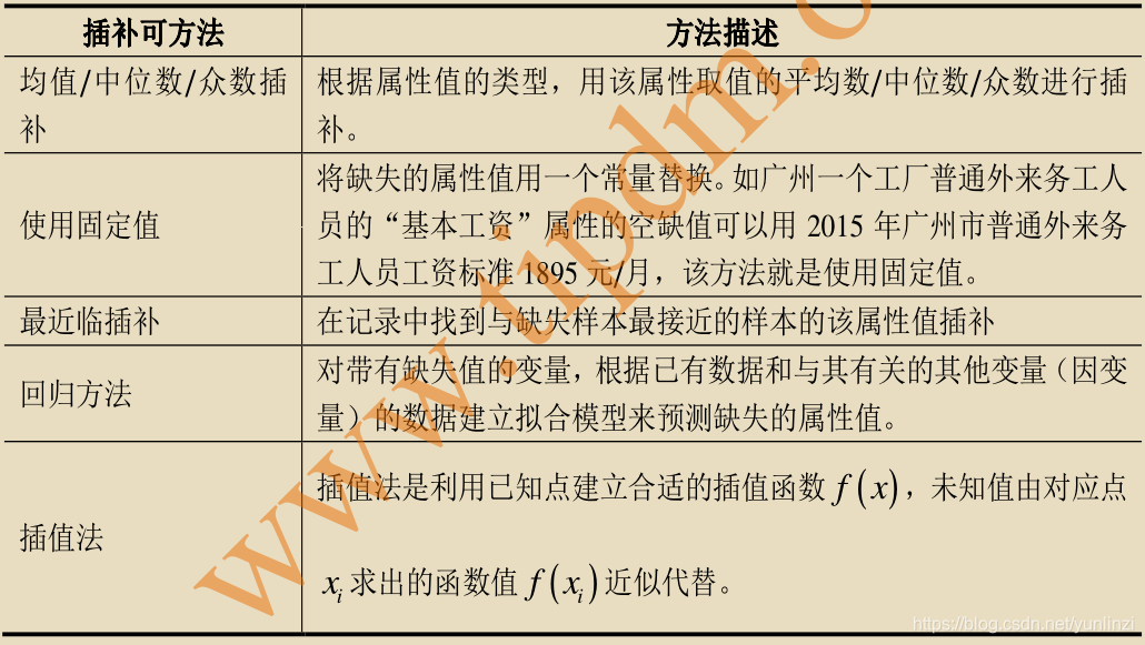
# 1. 数据可视化基础与重要性
在数据科学的世界里,数据可视化是将数据转化为图形和图表的实践过程,使得复杂的数据集可以通过直观的视觉形式来传达信息。它
ABB机器人在自动化生产线中是如何进行路径规划和任务执行的?请结合实际应用案例分析。
ABB机器人在自动化生产线中的应用广泛,其核心在于精确的路径规划和任务执行。路径规划是指机器人根据预定的目标位置和工作要求,计算出最优的移动轨迹。任务执行则涉及根据路径规划结果,控制机器人关节和运动部件精确地按照轨迹移动,完成诸如焊接、装配、搬运等任务。
参考资源链接:[ABB-机器人介绍.ppt](https://wenku.csdn.net/doc/7xfddv60ge?spm=1055.2569.3001.10343)
ABB机器人能够通过其先进的控制器和编程软件进行精确的路径规划。控制器通常使用专门的算法,如A*算法或者基于时间最优的轨迹规划技术,以确保机器人运动的平滑性和效率。此
网络物理突变工具的多点路径规划实现与分析
资源摘要信息:"多点路径规划matlab代码-mutationdocker:变异码头工人"
### 知识点概述
#### 多点路径规划与网络物理突变工具
多点路径规划指的是在网络环境下,对多个路径点进行规划的算法或工具。该工具可能被应用于物流、运输、通信等领域,以优化路径和提升效率。网络物理系统(CPS,Cyber-Physical System)结合了计算机网络和物理过程,其中网络物理突变工具是指能够修改或影响网络物理系统中的软件代码的功能,特别是在自动驾驶、智能电网、工业自动化等应用中。
#### 变异与Mutator软件工具
变异(Mutation)在软件测试领域是指故意对程序代码进行小的改动,以此来检测程序测试用例的有效性。mutator软件工具是一种自动化的工具,它能够在编程文件上执行这些变异操作。在代码质量保证和测试覆盖率的评估中,变异分析是提高软件可靠性的有效方法。
#### Mutationdocker
Mutationdocker是一个配置为运行mutator的虚拟机环境。虚拟机环境允许用户在隔离的环境中运行软件,无需对现有系统进行改变,从而保证了系统的稳定性和安全性。Mutationdocker的使用为开发者提供了一个安全的测试平台,可以在不影响主系统的情况下进行变异测试。
#### 工具的五个阶段
网络物理突变工具按照以下五个阶段进行操作:
1. **安装工具**:用户需要下载并构建工具,具体操作步骤可能包括解压文件、安装依赖库等。
2. **生成突变体**:使用`./mutator`命令,顺序执行`./runconfiguration`(如果存在更改的config.txt文件)、`make`和工具执行。这个阶段涉及到对原始程序代码的变异生成。
3. **突变编译**:该步骤可能需要编译运行环境的配置,依赖于项目具体情况,可能需要执行`compilerun.bash`脚本。
4. **突变执行**:通过`runsave.bash`脚本执行变异后的代码。这个脚本的路径可能需要根据项目进行相应的调整。
5. **结果分析**:利用MATLAB脚本对变异过程中的结果进行分析,可能需要参考文档中的文件夹结构部分,以正确引用和处理数据。
#### 系统开源
标签“系统开源”表明该项目是一个开放源代码的系统,意味着它被设计为可供任何人自由使用、修改和分发。开源项目通常可以促进协作、透明性以及通过社区反馈来提高代码质量。
#### 文件名称列表
文件名称列表中提到的`mutationdocker-master`可能是指项目源代码的仓库名,表明这是一个主分支,用户可以从中获取最新的项目代码和文件。
### 详细知识点
1. **多点路径规划**是网络物理系统中的一项重要技术,它需要考虑多个节点或路径点在物理网络中的分布,以及如何高效地规划它们之间的路径,以满足例如时间、成本、距离等优化目标。
2. **突变测试**是软件测试的一种技术,通过改变程序中的一小部分来生成变异体,这些变异体用于测试软件的测试用例集是否能够检测到这些人为的错误。如果测试用例集能够正确地识别出大多数或全部的变异体,那么可以认为测试用例集是有效的。
3. **Mutator软件工具**的使用可以自动化变异测试的过程,包括变异体的生成、编译、执行和结果分析。使用此类工具可以显著提高测试效率,尤其是在大型项目中。
4. **Mutationdocker的使用**提供了一个简化的环境,允许开发者无需复杂的配置就可以进行变异测试。它可能包括了必要的依赖项和工具链,以便快速开始变异测试。
5. **软件的五个操作阶段**为用户提供了清晰的指导,从安装到结果分析,每个步骤都有详细的说明,这有助于减少用户在使用过程中的困惑,并确保操作的正确性。
6. **开源系统的特性**鼓励了代码共享、共同开发和创新,同时也意味着用户可以通过社区的力量不断改进软件工具,这也是开源项目可持续发展的核心。
通过以上描述和知识点的展开,我们可以了解到多点路径规划matlab代码-mutationdocker:变异码头工人是一个涵盖了网络物理系统、变异测试、自动化软件工具以及开源精神的综合性项目。它通过一系列操作流程为用户提供了一个高效和稳定的代码测试环境,并且以开源的形式促进了软件测试技术的共享和创新。
"互动学习:行动中的多样性与论文攻读经历"
多样性她- 事实上SCI NCES你的时间表ECOLEDO C Tora SC和NCESPOUR l’Ingén学习互动,互动学习以行动为中心的强化学习学会互动,互动学习,以行动为中心的强化学习计算机科学博士论文于2021年9月28日在Villeneuve d'Asq公开支持马修·瑟林评审团主席法布里斯·勒菲弗尔阿维尼翁大学教授论文指导奥利维尔·皮耶昆谷歌研究教授:智囊团论文联合主任菲利普·普雷教授,大学。里尔/CRISTAL/因里亚报告员奥利维耶·西格德索邦大学报告员卢多维奇·德诺耶教授,Facebook /索邦大学审查员越南圣迈IMT Atlantic高级讲师邀请弗洛里安·斯特鲁布博士,Deepmind对于那些及时看到自己错误的人...3谢谢你首先,我要感谢我的两位博士生导师Olivier和Philippe。奥利维尔,"站在巨人的肩膀上"这句话对你来说完全有意义了。从科学上讲,你知道在这篇论文的(许多)错误中,你是我可以依
自动化缺失值处理脚本编写

# 1. 自动化缺失值处理概览
在数据科学的实践中,数据分析和建模的一个常见挑战是处理含有缺失值的数据集。缺失值不仅会降低数据的质量,而且可能会导致不准
SQLite在非易失性内存环境下如何进行事务处理和缓冲区管理的优化?
SQLite作为一种轻量级数据库系统,在面对非易失性内存(NVM)技术时,需要对传统的事务处理和缓冲区管理进行优化以充分利用NVM的优势。传统的SQLite设计在事务处理上存在较高的I/O开销,同时缓冲区管理方面存在空间浪费和并发性问题。随着NVM技术的发展,如Intel Optane DIMM,数据库架构需要相应的革新来适应新的存储特性。在这样的背景下,提出了SQLite-CC这一新型的缓冲区管理方案。
参考资源链接:[非易失性内存下的SQLite缓冲区管理:SQLite-CC](https://wenku.csdn.net/doc/1bbz2dtkc8?spm=1055.2569.300
multifeed: 实现多作者间的超核心共享与同步技术
资源摘要信息: "multifeed:多作者超核" 主要介绍了关于一个名为 "multifeed" 的模块,该模块在设计上支持多页进纸、多作者同步超核内容的功能。这个模块允许用户管理和同步一组超核(Hypercores),这是一类用于分布式数据存储的低级抽象。在该描述中,"超核"可以理解为一种分布式数据存储的核心单位,用于存储和同步数据。接下来,我们将详细探讨该模块的技术细节和用途。
### 知识点:
#### 1. 多页进纸的概念
"多页进纸"是一个形象的比喻,此处表示能够同时处理多个超核集合。在实际应用中,可能指的是同时操作或存储多个超核数据集,这在需要处理大规模分布式数据时十分有用。
#### 2. 超核(Hypercores)的定义
超核是分布式网络中的核心数据结构,它们能够存储和同步信息。一个超核可以被视为一个拥有唯一身份标识的数据存储单位,在分布式系统中,多个超核可以共同组成一个大型的分布式数据库。
#### 3. 超核集(Hypercore Set)
超核集是由多个超核组成的集合,可以被本地和远程系统访问。通过 "multifeed",用户可以管理多个这样的集合,实现高效的数据同步和管理。
#### 4. 远程超级核心集(Remote Supercore Set)
远程超级核心集指的是网络中其他节点上的超核集,它们可以通过网络连接到本地超核集。"multifeed" 让用户能够复制这些远程集到本地,实现数据共享和冗余。
#### 5. 复制机制(Replication Mechanism)
复制机制允许超核集在本地和远程之间进行数据同步。这里的复制机制是通过扩展传统的超核心交换机制实现的,加入了元交换(meta-exchange)的概念,即对等方之间共享本地提要信息并选择下载远程提要。
#### 6. 元交换机制
元交换是超核同步过程中的一个步骤,允许节点在同步数据时交换有关超核的信息,例如它们的内容和状态。这有助于节点之间更高效地决定哪些远程数据是值得下载的。
#### 7. JavaScript 编程语言的使用
"multifeed" 模块是用 JavaScript 编写的,这表明它可以在任何支持 Node.js 的环境中运行。由于 JavaScript 的普及和易用性,这为开发人员提供了一个灵活的方式来处理分布式数据。
#### 8. Random-access-memory(RAM)模块的使用
在 "multifeed" 示例代码中,使用了 "random-access-memory"(RAM)模块,这表明 "multifeed" 可以操作内存中的数据,这可能是实现快速读写操作的一种方式。
#### 9. Node.js 项目结构
从提供的示例代码和文件名称列表(multifeed-master)可以推测,"multifeed" 可能是一个 Node.js 项目,这意味着它可以在服务器端运行,执行后端任务,如文件存储、数据同步等。
#### 10. 使用场景和目的
"multifeed" 的设计目的是支持多作者环境下的超核同步,这使得它特别适合于需要多人协作的分布式系统。它通过控制多个作者对数据的访问权限,确保数据的一致性和完整性。
综上所述,"multifeed:多作者超核"是一个高级的分布式数据存储和同步解决方案,它利用了超核技术来为多用户协作提供支持,并且在技术上采用了类似元交换和远程数据复制的高级同步机制。该模块用JavaScript编写,易于集成到各种现代的Node.js应用中,并且能够处理大量数据,以支持大规模的协作和数据共享。