spi对flash连续写 verilog
时间: 2023-09-18 21:02:47 浏览: 55
SPI(Serial Peripheral Interface)是一种通信协议,用于在数字系统之间传输数据。在Verilog中通过SPI协议来实现对Flash的连续写入操作,需要以下几个步骤。
首先,需要定义SPI总线的输入和输出信号。输入信号通常包括时钟信号、数据输入信号、数据输出使能信号以及使能信号等。输出信号则通常包括数据输出信号。
接下来,在Verilog中编写SPI总线接口模块,实现数据的串行传输和数据的收发。可以使用状态机来处理SPI通信协议。
然后,需要定义Flash的接口,包括控制信号和数据信号。典型的控制信号包括写使能信号、写数据信号、写地址信号等。数据信号则用于存储要写入Flash的数据。
在连续写入操作中,首先需要发送写使能信号,使Flash进入写入模式。然后,通过SPI总线传输数据和地址,将数据写入到Flash的指定地址中。
在Verilog代码中,可以使用一个计数器来追踪写入的数据和地址数量。当计数器达到指定的数值时,表示连续写入完成。
最后,可以设计一个测试模块对SPI对Flash连续写入的Verilog代码进行验证。在测试模块中,可以模拟SPI总线发送数据和测试Flash读取数据的功能。
总结起来,SPI对Flash连续写入的Verilog实现需要定义SPI总线的输入输出信号,编写SPI总线接口模块和Flash接口模块,以及设计一个测试模块进行验证。通过以上步骤,可以实现对Flash的连续写入操作。
相关问题
spi flash 仿真模型 verilog
如果您需要使用Verilog进行SPI Flash的仿真模型开发,可以参考以下步骤:
1. 确定仿真模型的规格:您需要先确定您要仿真的SPI Flash的规格,例如容量、页大小、擦写块大小、时序等信息。
2. 编写Verilog代码:根据SPI Flash的规格,编写相应的Verilog代码,包括模块接口、状态机、读写逻辑、擦写逻辑等部分。
3. 进行仿真测试:使用Verilog仿真器进行仿真测试,验证代码的正确性和性能。您可以使用常用的Verilog仿真器,如ModelSim、Verilator等。
4. 集成到您的设计中:完成仿真测试后,您可以将SPI Flash的仿真模型集成到您的设计中,并与其他模块进行联调和测试。
需要注意的是,SPI Flash的仿真模型开发需要一定的Verilog编程经验和对SPI Flash的了解,如果您缺乏相关经验,可以考虑参考现有的SPI Flash仿真模型,或者寻求专业的Verilog开发服务。
verilog spi flash
Verilog is a hardware description language used for designing digital circuits. SPI (Serial Peripheral Interface) flash is a type of non-volatile memory used in embedded systems to store program code, configuration data, and user data.
To interface a Verilog design with an SPI flash, the Verilog code needs to communicate with the SPI flash using the SPI protocol. This involves sending and receiving data on the SPI bus, which consists of four signals: SCLK, MOSI, MISO, and SS.
The SCLK signal is the clock signal used to synchronize the data transfer between the Verilog design and the SPI flash. The MOSI signal is the Master Out Slave In signal, used to send data from the Verilog design to the SPI flash. The MISO signal is the Master In Slave Out signal, used to send data from the SPI flash to the Verilog design. The SS signal is the Slave Select signal, used to select the SPI flash for communication.
To interface with an SPI flash, the Verilog code needs to implement a SPI controller that can send and receive data on the SPI bus. The SPI controller needs to be able to send commands to the SPI flash to read, write, erase, or modify data stored in the flash memory.
Once the SPI controller is implemented in Verilog, it can be integrated into a larger design, such as a microcontroller or FPGA, to create an embedded system that can communicate with an SPI flash. This enables the system to store and retrieve data from the flash memory, which can be used for various purposes, such as booting the system, storing configuration data, or logging data.
相关推荐
最新推荐
FPGA作为从机与STM32进行SPI协议通信---Verilog实现
SPI,是英语Serial Peripheral Interface的缩写,顾名思义就是串行外围设备接口。SPI,是一种高速的,全双工,同步的通信总线,并且在芯片的管脚上只占用四根线,节约了芯片的管脚,同时为PCB的布局上节省空间,提供...
SPI串行总线接口的Verilog实现
详细描述了通过Verilog语言在FPGA中实现SPI逻辑的流程,文档中给出了代码。
起点小说解锁.js
起点小说解锁.js
RTL8188FU-Linux-v5.7.4.2-36687.20200602.tar(20765).gz
REALTEK 8188FTV 8188eus 8188etv linux驱动程序稳定版本, 支持AP,STA 以及AP+STA 共存模式。 稳定支持linux4.0以上内核。
管理建模和仿真的文件
管理Boualem Benatallah引用此版本:布阿利姆·贝纳塔拉。管理建模和仿真。约瑟夫-傅立叶大学-格勒诺布尔第一大学,1996年。法语。NNT:电话:00345357HAL ID:电话:00345357https://theses.hal.science/tel-003453572008年12月9日提交HAL是一个多学科的开放存取档案馆,用于存放和传播科学研究论文,无论它们是否被公开。论文可以来自法国或国外的教学和研究机构,也可以来自公共或私人研究中心。L’archive ouverte pluridisciplinaire
:YOLOv1目标检测算法:实时目标检测的先驱,开启计算机视觉新篇章
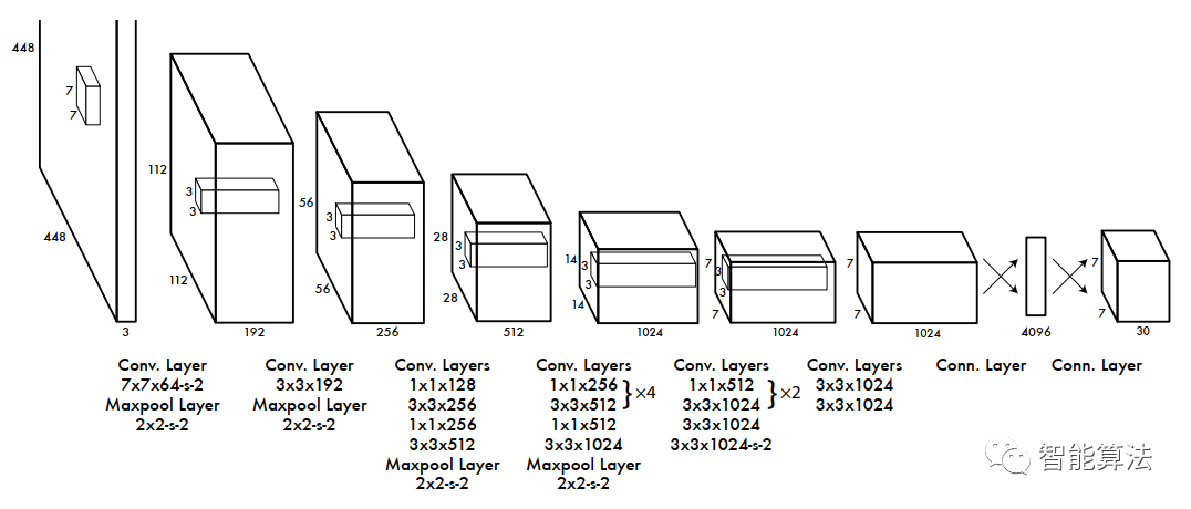
# 1. 目标检测算法概述
目标检测算法是一种计算机视觉技术,用于识别和定位图像或视频中的对象。它在各种应用中至关重要,例如自动驾驶、视频监控和医疗诊断。
目标检测算法通常分为两类:两阶段算法和单阶段算法。两阶段算法,如 R-CNN 和 Fast R-CNN,首先生成候选区域,然后对每个区域进行分类和边界框回归。单阶段算法,如 YOLO 和 SSD,一次性执行检
info-center source defatult
这是一个 Cisco IOS 命令,用于配置 Info Center 默认源。Info Center 是 Cisco 设备的日志记录和报告工具,可以用于收集和查看设备的事件、警报和错误信息。该命令用于配置 Info Center 默认源,即设备的默认日志记录和报告服务器。在命令行界面中输入该命令后,可以使用其他命令来配置默认源的 IP 地址、端口号和协议等参数。
c++校园超市商品信息管理系统课程设计说明书(含源代码) (2).pdf
校园超市商品信息管理系统课程设计旨在帮助学生深入理解程序设计的基础知识,同时锻炼他们的实际操作能力。通过设计和实现一个校园超市商品信息管理系统,学生掌握了如何利用计算机科学与技术知识解决实际问题的能力。在课程设计过程中,学生需要对超市商品和销售员的关系进行有效管理,使系统功能更全面、实用,从而提高用户体验和便利性。
学生在课程设计过程中展现了积极的学习态度和纪律,没有缺勤情况,演示过程流畅且作品具有很强的使用价值。设计报告完整详细,展现了对问题的深入思考和解决能力。在答辩环节中,学生能够自信地回答问题,展示出扎实的专业知识和逻辑思维能力。教师对学生的表现予以肯定,认为学生在课程设计中表现出色,值得称赞。
整个课程设计过程包括平时成绩、报告成绩和演示与答辩成绩三个部分,其中平时表现占比20%,报告成绩占比40%,演示与答辩成绩占比40%。通过这三个部分的综合评定,最终为学生总成绩提供参考。总评分以百分制计算,全面评估学生在课程设计中的各项表现,最终为学生提供综合评价和反馈意见。
通过校园超市商品信息管理系统课程设计,学生不仅提升了对程序设计基础知识的理解与应用能力,同时也增强了团队协作和沟通能力。这一过程旨在培养学生综合运用技术解决问题的能力,为其未来的专业发展打下坚实基础。学生在进行校园超市商品信息管理系统课程设计过程中,不仅获得了理论知识的提升,同时也锻炼了实践能力和创新思维,为其未来的职业发展奠定了坚实基础。
校园超市商品信息管理系统课程设计的目的在于促进学生对程序设计基础知识的深入理解与掌握,同时培养学生解决实际问题的能力。通过对系统功能和用户需求的全面考量,学生设计了一个实用、高效的校园超市商品信息管理系统,为用户提供了更便捷、更高效的管理和使用体验。
综上所述,校园超市商品信息管理系统课程设计是一项旨在提升学生综合能力和实践技能的重要教学活动。通过此次设计,学生不仅深化了对程序设计基础知识的理解,还培养了解决实际问题的能力和团队合作精神。这一过程将为学生未来的专业发展提供坚实基础,使其在实际工作中能够胜任更多挑战。
"互动学习:行动中的多样性与论文攻读经历"
多样性她- 事实上SCI NCES你的时间表ECOLEDO C Tora SC和NCESPOUR l’Ingén学习互动,互动学习以行动为中心的强化学习学会互动,互动学习,以行动为中心的强化学习计算机科学博士论文于2021年9月28日在Villeneuve d'Asq公开支持马修·瑟林评审团主席法布里斯·勒菲弗尔阿维尼翁大学教授论文指导奥利维尔·皮耶昆谷歌研究教授:智囊团论文联合主任菲利普·普雷教授,大学。里尔/CRISTAL/因里亚报告员奥利维耶·西格德索邦大学报告员卢多维奇·德诺耶教授,Facebook /索邦大学审查员越南圣迈IMT Atlantic高级讲师邀请弗洛里安·斯特鲁布博士,Deepmind对于那些及时看到自己错误的人...3谢谢你首先,我要感谢我的两位博士生导师Olivier和Philippe。奥利维尔,"站在巨人的肩膀上"这句话对你来说完全有意义了。从科学上讲,你知道在这篇论文的(许多)错误中,你是我可以依
:YOLO目标检测算法的挑战与机遇:数据质量、计算资源与算法优化,探索未来发展方向
# 1. YOLO目标检测算法简介
YOLO(You Only Look Once)是一种