module set(clk,rst,entry, o_tag,writedata,byte_en,write,word_en,readdata,wb_addr, hit,modify, miss,valid,read_miss); parameter cache_entry = 14; input wire clk, rst; input wire [cache_entry-1:0] entry; input wire [22-cache_entry:0] o_tag; input wire [127:0] writedata; input wire [3:0] byte_en; input wire read_miss; input wire write; input wire [3:0] word_en; output wire [127:0] readdata; output wire [22:0] wb_addr; output wire hit, modify, miss, valid; wire [22-cache_entry:0] i_tag; wire dirty; wire [24-cache_entry:0] write_tag_data;
时间: 2024-04-20 19:25:25 浏览: 77

FIFO.rar_fifo vhdl
这段代码是一个cache模块的定义,它包含一些输入和输出信号。其中,clk和rst是时钟和复位信号,entry是指定要访问的cache条目的索引,o_tag是访问地址的标签部分,writedata是要写入cache的数据,byte_en是指定写入字节的使能位,read_miss是读取操作是否发生缺失的信号,write是写入操作的使能信号,word_en指定读取操作的字节使能位。输出信号包括readdata表示从cache读取的数据,wb_addr表示要写回的地址,hit表示是否命中,modify表示是否需要修改,miss表示是否发生缺失,valid表示cache条目是否有效。还定义了一些内部信号i_tag、dirty和write_tag_data。
阅读全文
相关推荐
最新推荐
同步FIFO和异步FIFO的Verilog实现
`always @(posedge clk or negedge rst)`块用于处理时钟边沿触发的事件,`if(wr && ~full_in) mem[wp]<=datain;`这一行代码表示在没有满状态并且写使能有效时,将数据写入内存。`full_in`和`empty_in`的生成通过两个...
YOLO算法-城市电杆数据集-496张图像带标签-电杆.zip
YOLO系列算法目标检测数据集,包含标签,可以直接训练模型和验证测试,数据集已经划分好,包含数据集配置文件data.yaml,适用yolov5,yolov8,yolov9,yolov7,yolov10,yolo11算法;
包含两种标签格:yolo格式(txt文件)和voc格式(xml文件),分别保存在两个文件夹中,文件名末尾是部分类别名称;
yolo格式:<class> <x_center> <y_center> <width> <height>, 其中:
<class> 是目标的类别索引(从0开始)。
<x_center> 和 <y_center> 是目标框中心点的x和y坐标,这些坐标是相对于图像宽度和高度的比例值,范围在0到1之间。
<width> 和 <height> 是目标框的宽度和高度,也是相对于图像宽度和高度的比例值;
【注】可以下拉页面,在资源详情处查看标签具体内容;
Java毕业设计项目:校园二手交易网站开发指南
资源摘要信息:"Java是一种高性能、跨平台的面向对象编程语言,由Sun Microsystems(现为Oracle Corporation)的James Gosling等人在1995年推出。其设计理念是为了实现简单性、健壮性、可移植性、多线程以及动态性。Java的核心优势包括其跨平台特性,即“一次编写,到处运行”(Write Once, Run Anywhere),这得益于Java虚拟机(JVM)的存在,它提供了一个中介,使得Java程序能够在任何安装了相应JVM的设备上运行,无论操作系统如何。
Java是一种面向对象的编程语言,这意味着它支持面向对象编程(OOP)的三大特性:封装、继承和多态。封装使得代码模块化,提高了安全性;继承允许代码复用,简化了代码的复杂性;多态则增强了代码的灵活性和扩展性。
Java还具有内置的多线程支持能力,允许程序同时处理多个任务,这对于构建服务器端应用程序、网络应用程序等需要高并发处理能力的应用程序尤为重要。
自动内存管理,特别是垃圾回收机制,是Java的另一大特性。它自动回收不再使用的对象所占用的内存资源,这样程序员就无需手动管理内存,从而减轻了编程的负担,并减少了因内存泄漏而导致的错误和性能问题。
Java广泛应用于企业级应用开发、移动应用开发(尤其是Android平台)、大型系统开发等领域,并且有大量的开源库和框架支持,例如Spring、Hibernate、Struts等,这些都极大地提高了Java开发的效率和质量。
标签中提到的Java、毕业设计、课程设计和开发,意味着文件“毕业设计---社区(校园)二手交易网站.zip”中的内容可能涉及到Java语言的编程实践,可能是针对学生的课程设计或毕业设计项目,而开发则指出了这些内容的具体活动。
在文件名称列表中,“SJT-code”可能是指该压缩包中包含的是一个特定的项目代码,即社区(校园)二手交易网站的源代码。这类网站通常需要实现用户注册、登录、商品发布、浏览、交易、评价等功能,并且需要后端服务器支持,如数据库连接和事务处理等。考虑到Java的特性,网站的开发可能使用了Java Web技术栈,如Servlet、JSP、Spring Boot等,以及数据库技术,如MySQL或MongoDB等。"
管理建模和仿真的文件
管理Boualem Benatallah引用此版本:布阿利姆·贝纳塔拉。管理建模和仿真。约瑟夫-傅立叶大学-格勒诺布尔第一大学,1996年。法语。NNT:电话:00345357HAL ID:电话:00345357https://theses.hal.science/tel-003453572008年12月9日提交HAL是一个多学科的开放存取档案馆,用于存放和传播科学研究论文,无论它们是否被公开。论文可以来自法国或国外的教学和研究机构,也可以来自公共或私人研究中心。L’archive ouverte pluridisciplinaire
【MVC标准化:肌电信号处理的终极指南】:提升数据质量的10大关键步骤与工具
# 摘要
MVC标准化是肌电信号处理中确保数据质量的重要步骤,它对于提高测量结果的准确性和可重复性至关重要。本文首先介绍肌电信号的生理学原理和MVC标准化理论,阐述了数据质量的重要性及影响因素。随后,文章深入探讨了肌电信号预处理的各个环节,包括噪声识别与消除、信号放大与滤波技术、以及基线漂移的校正方法。在提升数据质量的关键步骤部分,本文详细描述了信号特征提取、MVC标准化的实施与评估,并讨论了数据质量评估与优化工具。最后,本文通过实验设计和案例分析,展示了MVC标准化在实践应用中的具
能否提供一个在R语言中执行Framingham数据集判别分析的详细和完整的代码示例?
当然可以。在R语言中,Framingham数据集是一个用于心血管疾病研究的经典数据集。以下是使用`ggfortify`包结合` factoextra`包进行判别分析的一个基本步骤:
首先,你需要安装所需的库,如果尚未安装,可以使用以下命令:
```r
install.packages(c("ggfortify", "factoextra"))
```
然后加载所需的数据集并做预处理。Framingham数据集通常存储在`MASS`包中,你可以通过下面的代码加载:
```r
library(MASS)
data(Framingham)
```
接下来,我们假设你已经对数据进行了适当的清洗和转换
Blaseball Plus插件开发与构建教程
资源摘要信息:"Blaseball Plus"
Blaseball Plus是一个与游戏Blaseball相关的扩展项目,该项目提供了一系列扩展和改进功能,以增强Blaseball游戏体验。在这个项目中,JavaScript被用作主要开发语言,通过在package.json文件中定义的脚本来完成构建任务。项目说明中提到了开发环境的要求,即在20.09版本上进行开发,并且提供了一个flake.nix文件来复制确切的构建环境。虽然Nix薄片是一项处于工作状态(WIP)的功能且尚未完全记录,但可能需要用户自行安装系统依赖项,其中列出了Node.js和纱(Yarn)的特定版本。
### 知识点详细说明:
#### 1. Blaseball游戏:
Blaseball是一个虚构的棒球游戏,它在互联网社区中流行,其特点是独特的规则、随机事件和社区参与的元素。
#### 2. 扩展开发:
Blaseball Plus是一个扩展,它可能是为在浏览器中运行的Blaseball游戏提供额外功能和改进的软件。扩展开发通常涉及编写额外的代码来增强现有软件的功能。
#### 3. JavaScript编程语言:
JavaScript是一种高级的、解释执行的编程语言,被广泛用于网页和Web应用的客户端脚本编写,是开发Web扩展的关键技术之一。
#### 4. package.json文件:
这是Node.js项目的核心配置文件,用于声明项目的各种配置选项,包括项目名称、版本、依赖关系以及脚本命令等。
#### 5.构建脚本:
描述中提到的脚本,如`build:dev`、`build:prod:unsigned`和`build:prod:signed`,这些脚本用于自动化构建过程,可能包括编译、打包、签名等步骤。`yarn run`命令用于执行这些脚本。
#### 6. yarn包管理器:
Yarn是一个快速、可靠和安全的依赖项管理工具,类似于npm(Node.js的包管理器)。它允许开发者和项目管理依赖项,通过简单的命令行界面可以轻松地安装和更新包。
#### 7. Node.js版本管理:
项目要求Node.js的具体版本,这里是14.9.0版本。管理特定的Node.js版本是重要的,因为在不同版本间可能会存在API变化或其他不兼容问题,这可能会影响扩展的构建和运行。
#### 8. 系统依赖项的安装:
文档提到可能需要用户手动安装系统依赖项,这在使用Nix薄片时尤其常见。Nix薄片(Nix flakes)是一个实验性的Nix特性,用于提供可复现的开发环境和构建设置。
#### 9. Web扩展的工件放置:
构建后的工件放置在`addon/web-ext-artifacts/`目录中,表明这可能是一个基于WebExtension的扩展项目。WebExtension是一种跨浏览器的扩展API,用于创建浏览器扩展。
#### 10. 扩展部署:
描述中提到了两种不同类型的构建版本:开发版(dev)和生产版(prod),其中生产版又分为未签名(unsigned)和已签名(signed)版本。这些不同的构建版本用于不同阶段的开发和发布。
通过这份文档,我们能够了解到Blaseball Plus项目的开发环境配置、构建脚本的使用、依赖管理工具的运用以及Web扩展的基本概念和部署流程。这些知识点对于理解JavaScript项目开发和扩展构建具有重要意义。
"互动学习:行动中的多样性与论文攻读经历"
多样性她- 事实上SCI NCES你的时间表ECOLEDO C Tora SC和NCESPOUR l’Ingén学习互动,互动学习以行动为中心的强化学习学会互动,互动学习,以行动为中心的强化学习计算机科学博士论文于2021年9月28日在Villeneuve d'Asq公开支持马修·瑟林评审团主席法布里斯·勒菲弗尔阿维尼翁大学教授论文指导奥利维尔·皮耶昆谷歌研究教授:智囊团论文联合主任菲利普·普雷教授,大学。里尔/CRISTAL/因里亚报告员奥利维耶·西格德索邦大学报告员卢多维奇·德诺耶教授,Facebook /索邦大学审查员越南圣迈IMT Atlantic高级讲师邀请弗洛里安·斯特鲁布博士,Deepmind对于那些及时看到自己错误的人...3谢谢你首先,我要感谢我的两位博士生导师Olivier和Philippe。奥利维尔,"站在巨人的肩膀上"这句话对你来说完全有意义了。从科学上讲,你知道在这篇论文的(许多)错误中,你是我可以依
【天线性能提升密籍】:深入探究均匀线阵方向图设计原则及案例分析
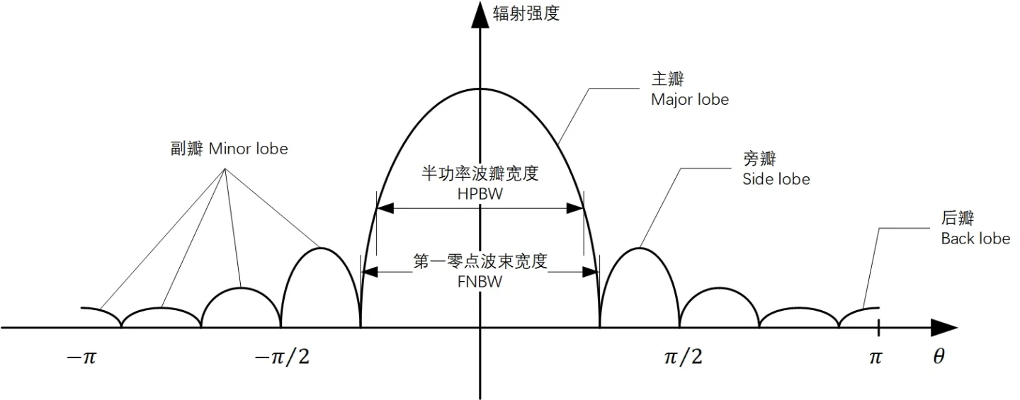
# 摘要
本文深入探讨了均匀线阵天线的基础理论及其方向图设计,旨在提升天线系统的性能和应用效能。文章首先介绍了均匀线阵及方向图的基本概念,并阐述了方向图设计的理论基础,包括波束形成与主瓣及副瓣特性的控制。随后,论文通过设计软件工具的应用和实际天线系统调试方法,展示了方向图设计的实践技巧。文中还包含了一系列案例分析,以实证研究验证理论,并探讨了均匀线阵性能
C#怎么把图片存入名为当前日期的文件夹里
在C#中,你可以通过`System.IO`命名空间下的`Directory`和`File`类来创建并存储图片到包含当前日期的文件夹里。以下是一个简单的示例:
```csharp
using System;
using System.IO;
public void SaveImageToTodayFolder(string imagePath, string imageName)
{
// 获取当前日期
DateTime currentDate = DateTime.Now;
string folderPath = Path.Combine(Environment.C