sdram和flash fpga
时间: 2023-09-20 20:08:56 浏览: 43
SDRAM和Flash是两种不同类型的存储器,都可以用于FPGA中。
SDRAM(Synchronous Dynamic Random Access Memory)是一种同步动态随机存取存储器,可以高速读写数据。它通常用于存储大量的数据,如图像、音频和视频等。SDRAM可以被FPGA作为外部存储器使用,可以通过FPGA的外部接口控制读写操作。
Flash是一种非易失性存储器,可以长期存储数据而不需要电源支持。它通常用于存储程序代码和配置文件等数据。FPGA中的Flash通常用于存储FPGA的配置文件,以便在上电时加载FPGA配置。
在FPGA设计中,SDRAM和Flash都可以用于存储数据和程序,但它们在性能、容量和使用方式等方面有所不同。在选择存储器时,需要根据具体应用场景来选择适合的存储器。
相关问题
fpga ddr sdram flash
FPGA (Field-Programmable Gate Array) is a type of integrated circuit that can be programmed after manufacturing. It is used to implement various digital circuits and systems, and it is highly configurable and flexible.
DDR (Double Data Rate) SDRAM (Synchronous Dynamic Random-Access Memory) is a type of memory used in computers and other digital devices. It allows for faster data transfer rates by transferring data on both the rising and falling edges of the clock signal.
Flash memory is a type of non-volatile memory that can be electrically erased and reprogrammed. It is commonly used in storage devices such as USB drives, memory cards, and solid-state drives.
All three of these technologies can be used together in various digital systems. For example, an FPGA can be used to implement the control logic for a system that uses DDR SDRAM for volatile memory and flash memory for non-volatile storage.
fpga读取spi flash的数据程序
FPGA是一种可编程逻辑芯片,它具有高度灵活性和可重构性,能够通过编程来实现不同的功能。SPI Flash是一种常用的存储器,可以通过SPI总线与FPGA进行通信。
FPGA读取SPI Flash的数据程序主要分为以下几个步骤:
1.设置SPI Flash通信参数。包括SPI时序设置、Flash对应的器件类型和容量等。
2.从SPI Flash读取数据。首先,通过控制SPI总线的CLK、MOSI、MISO和SS等信号选择Flash,并向Flash发送命令,让Flash开始返回数据;然后,FPGA不断地向SPI总线发送时钟信号,同时用MOSI读取Flash传送的数据,直到读取完毕。
3.将读取的数据存储到FPGA内部存储器中。在读取过程中,FPGA可以使用内部的缓存寄存器来存储数据,也可以直接将数据写入SRAM或SDRAM等内部存储器中。
4.对读取的数据进行处理。FPGA读取的数据可以用于各种不同的应用,例如数据处理、控制逻辑等。
需要注意的是,FPGA读取SPI Flash的数据程序需要根据具体的应用场景进行调整和优化,考虑到SPI Flash的容量、读写速度、信号稳定性等因素,以确保读取的数据准确无误、高效稳定。
相关推荐
最新推荐
关于在FPGA上建立SOPC的教程
4.3 ModelSim和Quartus Ⅱ联合使用 40 第5章 基于FPGA的DSP开发技术 41 5.1Matlab/DSP builder及其设计流程 41 5.2DSP Builder的安装与注册 42 5.3基于MATLAB/Simulink模块的FIR滤波器设计与仿真 42 5.3基于IP核的...
RTL8188FU-Linux-v5.7.4.2-36687.20200602.tar(20765).gz
REALTEK 8188FTV 8188eus 8188etv linux驱动程序稳定版本, 支持AP,STA 以及AP+STA 共存模式。 稳定支持linux4.0以上内核。
管理建模和仿真的文件
管理Boualem Benatallah引用此版本:布阿利姆·贝纳塔拉。管理建模和仿真。约瑟夫-傅立叶大学-格勒诺布尔第一大学,1996年。法语。NNT:电话:00345357HAL ID:电话:00345357https://theses.hal.science/tel-003453572008年12月9日提交HAL是一个多学科的开放存取档案馆,用于存放和传播科学研究论文,无论它们是否被公开。论文可以来自法国或国外的教学和研究机构,也可以来自公共或私人研究中心。L’archive ouverte pluridisciplinaire
:YOLOv1目标检测算法:实时目标检测的先驱,开启计算机视觉新篇章
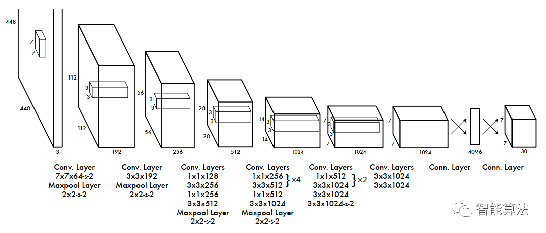
# 1. 目标检测算法概述
目标检测算法是一种计算机视觉技术,用于识别和定位图像或视频中的对象。它在各种应用中至关重要,例如自动驾驶、视频监控和医疗诊断。
目标检测算法通常分为两类:两阶段算法和单阶段算法。两阶段算法,如 R-CNN 和 Fast R-CNN,首先生成候选区域,然后对每个区域进行分类和边界框回归。单阶段算法,如 YOLO 和 SSD,一次性执行检
ActionContext.getContext().get()代码含义
ActionContext.getContext().get() 是从当前请求的上下文对象中获取指定的属性值的代码。在ActionContext.getContext()方法的返回值上,调用get()方法可以获取当前请求中指定属性的值。
具体来说,ActionContext是Struts2框架中的一个类,它封装了当前请求的上下文信息。在这个上下文对象中,可以存储一些请求相关的属性值,比如请求参数、会话信息、请求头、应用程序上下文等等。调用ActionContext.getContext()方法可以获取当前请求的上下文对象,而调用get()方法可以获取指定属性的值。
例如,可以使用 Acti
c++校园超市商品信息管理系统课程设计说明书(含源代码) (2).pdf
校园超市商品信息管理系统课程设计旨在帮助学生深入理解程序设计的基础知识,同时锻炼他们的实际操作能力。通过设计和实现一个校园超市商品信息管理系统,学生掌握了如何利用计算机科学与技术知识解决实际问题的能力。在课程设计过程中,学生需要对超市商品和销售员的关系进行有效管理,使系统功能更全面、实用,从而提高用户体验和便利性。
学生在课程设计过程中展现了积极的学习态度和纪律,没有缺勤情况,演示过程流畅且作品具有很强的使用价值。设计报告完整详细,展现了对问题的深入思考和解决能力。在答辩环节中,学生能够自信地回答问题,展示出扎实的专业知识和逻辑思维能力。教师对学生的表现予以肯定,认为学生在课程设计中表现出色,值得称赞。
整个课程设计过程包括平时成绩、报告成绩和演示与答辩成绩三个部分,其中平时表现占比20%,报告成绩占比40%,演示与答辩成绩占比40%。通过这三个部分的综合评定,最终为学生总成绩提供参考。总评分以百分制计算,全面评估学生在课程设计中的各项表现,最终为学生提供综合评价和反馈意见。
通过校园超市商品信息管理系统课程设计,学生不仅提升了对程序设计基础知识的理解与应用能力,同时也增强了团队协作和沟通能力。这一过程旨在培养学生综合运用技术解决问题的能力,为其未来的专业发展打下坚实基础。学生在进行校园超市商品信息管理系统课程设计过程中,不仅获得了理论知识的提升,同时也锻炼了实践能力和创新思维,为其未来的职业发展奠定了坚实基础。
校园超市商品信息管理系统课程设计的目的在于促进学生对程序设计基础知识的深入理解与掌握,同时培养学生解决实际问题的能力。通过对系统功能和用户需求的全面考量,学生设计了一个实用、高效的校园超市商品信息管理系统,为用户提供了更便捷、更高效的管理和使用体验。
综上所述,校园超市商品信息管理系统课程设计是一项旨在提升学生综合能力和实践技能的重要教学活动。通过此次设计,学生不仅深化了对程序设计基础知识的理解,还培养了解决实际问题的能力和团队合作精神。这一过程将为学生未来的专业发展提供坚实基础,使其在实际工作中能够胜任更多挑战。
"互动学习:行动中的多样性与论文攻读经历"
多样性她- 事实上SCI NCES你的时间表ECOLEDO C Tora SC和NCESPOUR l’Ingén学习互动,互动学习以行动为中心的强化学习学会互动,互动学习,以行动为中心的强化学习计算机科学博士论文于2021年9月28日在Villeneuve d'Asq公开支持马修·瑟林评审团主席法布里斯·勒菲弗尔阿维尼翁大学教授论文指导奥利维尔·皮耶昆谷歌研究教授:智囊团论文联合主任菲利普·普雷教授,大学。里尔/CRISTAL/因里亚报告员奥利维耶·西格德索邦大学报告员卢多维奇·德诺耶教授,Facebook /索邦大学审查员越南圣迈IMT Atlantic高级讲师邀请弗洛里安·斯特鲁布博士,Deepmind对于那些及时看到自己错误的人...3谢谢你首先,我要感谢我的两位博士生导师Olivier和Philippe。奥利维尔,"站在巨人的肩膀上"这句话对你来说完全有意义了。从科学上讲,你知道在这篇论文的(许多)错误中,你是我可以依
:YOLO目标检测算法的挑战与机遇:数据质量、计算资源与算法优化,探索未来发展方向
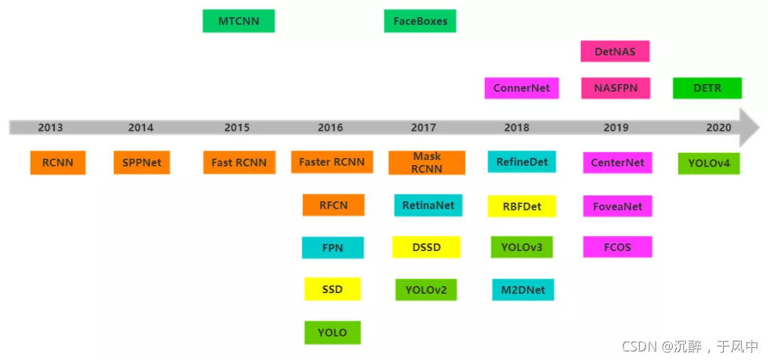
# 1. YOLO目标检测算法简介
YOLO(You Only Look Once)是一种
设计一个算法,输出在顺序表{3,6,2,10,1,8,5,7,4,9}中采用顺序方法查找关键字5的过程。
好的,我来回答你的问题。
在顺序表中查找关键字5的过程如下:
1. 从顺序表的第一个元素(即3)开始,逐个比较元素的值与目标值5是否相等。
2. 发现第一个元素3不等于目标值5,继续向下查找。
3. 查找到第三个元素2时,发现该元素也不等于目标值5,继续向下查找。
4. 查找到第四个元素10时,发现该元素也不等于目标值5,继续向下查找。
5. 查找到第五个元素1时,发现该元素也不等于目标值5,继续向下查找。
6. 查找到第六个元素8时,发现该元素也不等于目标值5,继续向下查找。
7. 查找到第七个元素5时,发现该元素等于目标值5,查找成功。
因此,顺序表中采用顺序方法查找关键
建筑供配电系统相关课件.pptx
建筑供配电系统是建筑中的重要组成部分,负责为建筑内的设备和设施提供电力支持。在建筑供配电系统相关课件中介绍了建筑供配电系统的基本知识,其中提到了电路的基本概念。电路是电流流经的路径,由电源、负载、开关、保护装置和导线等组成。在电路中,涉及到电流、电压、电功率和电阻等基本物理量。电流是单位时间内电路中产生或消耗的电能,而电功率则是电流在单位时间内的功率。另外,电路的工作状态包括开路状态、短路状态和额定工作状态,各种电气设备都有其额定值,在满足这些额定条件下,电路处于正常工作状态。而交流电则是实际电力网中使用的电力形式,按照正弦规律变化,即使在需要直流电的行业也多是通过交流电整流获得。
建筑供配电系统的设计和运行是建筑工程中一个至关重要的环节,其正确性和稳定性直接关系到建筑物内部设备的正常运行和电力安全。通过了解建筑供配电系统的基本知识,可以更好地理解和应用这些原理,从而提高建筑电力系统的效率和可靠性。在课件中介绍了电工基本知识,包括电路的基本概念、电路的基本物理量和电路的工作状态。这些知识不仅对电气工程师和建筑设计师有用,也对一般人了解电力系统和用电有所帮助。
值得一提的是,建筑供配电系统在建筑工程中的重要性不仅仅是提供电力支持,更是为了确保建筑物的安全性。在建筑供配电系统设计中必须考虑到保护装置的设置,以确保电路在发生故障时及时切断电源,避免潜在危险。此外,在电气设备的选型和布置时也需要根据建筑的特点和需求进行合理规划,以提高电力系统的稳定性和安全性。
在实际应用中,建筑供配电系统的设计和建设需要考虑多个方面的因素,如建筑物的类型、规模、用途、电力需求、安全标准等。通过合理的设计和施工,可以确保建筑供配电系统的正常运行和安全性。同时,在建筑供配电系统的维护和管理方面也需要重视,定期检查和维护电气设备,及时发现和解决问题,以确保建筑物内部设备的正常使用。
总的来说,建筑供配电系统是建筑工程中不可或缺的一部分,其重要性不言而喻。通过学习建筑供配电系统的相关知识,可以更好地理解和应用这些原理,提高建筑电力系统的效率和可靠性,确保建筑物内部设备的正常运行和电力安全。建筑供配电系统的设计、建设、维护和管理都需要严谨细致,只有这样才能确保建筑物的电力系统稳定、安全、高效地运行。