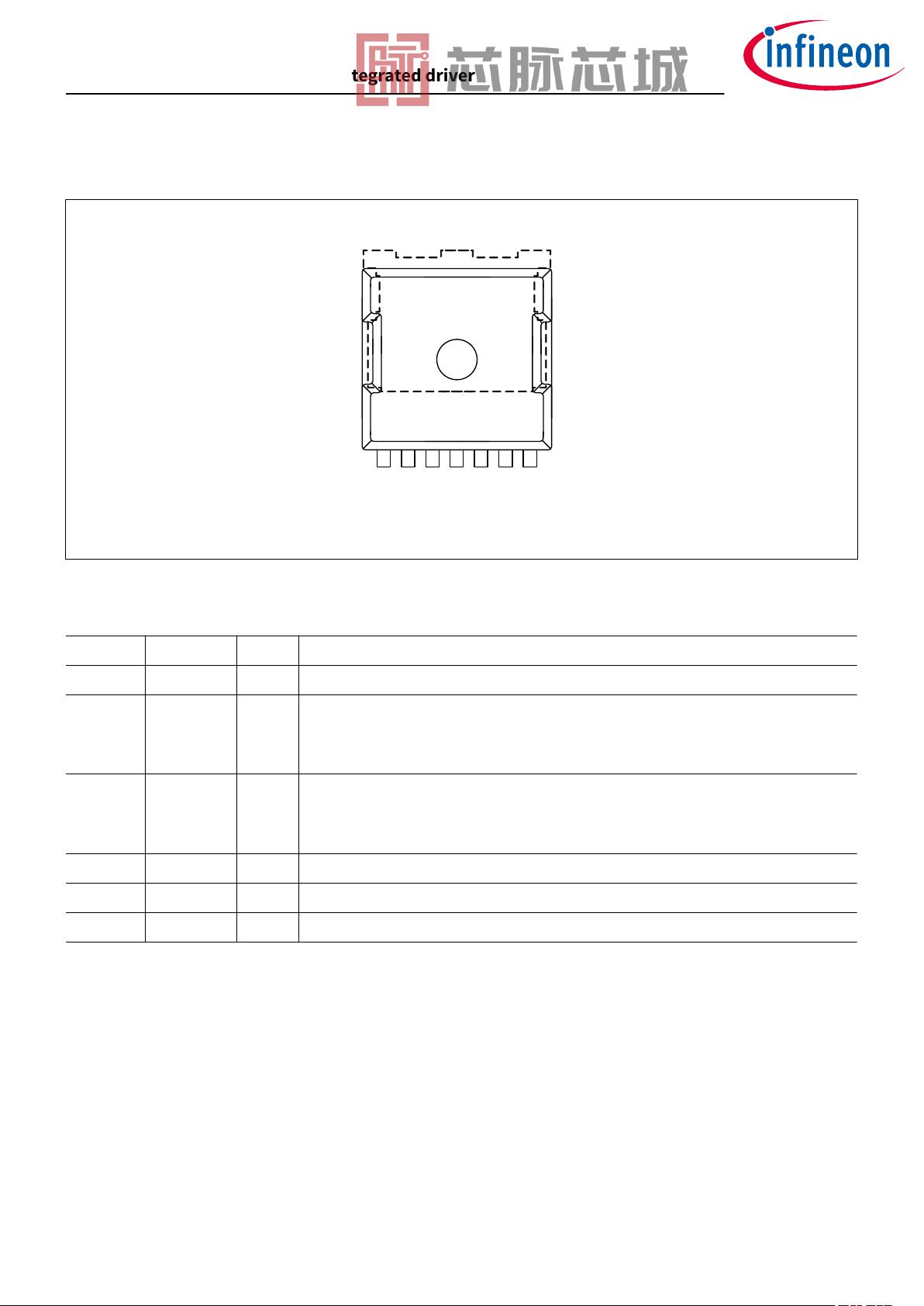
没有合适的资源?快使用搜索试试~ 我知道了~
首页英飞凌BTN9970LV芯片中文版规格书。
英飞凌BTN9970LV芯片中文版规格书。
需积分: 5 0 下载量 51 浏览量
更新于2023-11-23
收藏 637KB PDF 举报
BTN9970LV是一款英飞凌芯片。它是一款具有集成驱动器的高电流PN半桥。以下是该芯片的主要特点: 1. 符合AEC-Q100/Q006标准,达到1级质量要求。 2. 工作电压范围为8V至18V(最高可达40V)。 3. 在25°C下,通路阻抗为9.7mΩ(最高可达150°C下的18.1mΩ)。 4. 在85°C下的最大静态电流为3.3µA。 5. 具有过流、欠压和过温保护功能。 6. 最小过流检测电平为60A。 7. 具有8个可选择的开关斜升速率,以优化电磁干扰。 8. 状态标志诊断功能,可反馈电流感应、温度和斜升速率。 9. 封装标记为PG-HSOF-7-1。 BTN9970LV芯片适用于以下应用领域: 1. 汽车12V刷式直流电机。 2. 燃油泵。 3. 电动升降门。 4. 暖通空调风扇。 在电路方面,该芯片需要与微控制器(Micro-controller)连接,并且具有反向极性保护。此外,还有连接电容、电阻、二极管和电阻以及电流传感器等元件。 总的来说,BTN9970LV是一款功能强大的芯片,具有高电流和集成驱动器的特点。它在汽车和电动设备领域有着广泛的应用前景。
资源详情
资源推荐
![](https://csdnimg.cn/release/download_crawler_static/88054429/bg6.jpg)
2 Pin configuration
1
2
3
4
5
6
7
8
Figure 4 Pin assignment BTN9970LV (top view)
Table 1 Pin definitions and functions
Pin Symbol I/O Function
1,2 GND – Ground
(1)
3 IN I Input
Defines whether high- or low-side switch is activated.
An internal pull down resistor is connected to this pin.
4 INH I Inhibit
When set to low device goes in tristate.
An internal pull down resistor is connected to this pin.
5 IS O Current sense, temperature sense, slew rate level and diagnostics
6,7 VS – Supply
(1)
8 (EP) OUT O Power output of the bridge
1) All terminal pins must be connected together on the PCB. All terminal pins are internally connected together.
PCB traces have to be designed to withstand the maximum current which can flow
Bold type: pin needs power wiring
BTN9970LV NovalithIC
™
+
High current PN half-bridge with integrated driver
2 Pin configuration
Datasheet 6 Rev. 1.0
2021-10-12
![](https://csdnimg.cn/release/download_crawler_static/88054429/bg7.jpg)
3 General product characteristics
The device is intended to be used in an automotive environment. The circumstances, how the device
environment must look like, are described in this chapter.
3.1 Absolute maximum ratings
Stresses above the ones listed here may cause permanent damage to the device. Exposure to absolute
maximum rating conditions for extended periods may aect device reliability.
Table 2 Absolute Maximum Ratings
T
j
= -40°C to 150°C; all voltages with respect to ground, positive current flowing into pin (unless otherwise
specified)
1)
Parameter Symbol Values Unit Note or condition
Min. Typ. Max.
Voltages
Supply voltage V
S
-0.3 – 40 V –
Drain-source voltage high-side V
DS(HS)
-40 – – V T
j
≥ 25°C
Drain-source voltage high-side V
DS(HS)
-38 – – V T
j
< 25°C
Drain-source voltage low-side V
DS(LS)
– – 40 V T
j
≥ 25°C
Drain-source voltage low-side V
DS(LS)
– – 38 V T
j
< 25°C
Logic input voltage V
IN
V
INH
-0.3 – 5.5 V –
Voltage between VS and IS pin V
SIS
-0.3 – 40 V –
Voltage at IS pin V
IS
-0.3 – 40 V –
Currents
HS drain current |I
D(HS)
| – – I
OCH0
A Switch active
2)
LS drain current |I
D(LS)
| – – I
OCL0
A Switch active
2)
Temperatures
Junction temperature T
j
-40 – 150 °C –
Storage temperature T
stg
-55 – 150 °C –
ESD susceptibility
ESD robustness all pins (HBM) |V
ESD(HBM,local)
| – – 2 kV HBM
3)
ESD robustness OUT vs GND
vs VS (HBM)
|V
ESD(HBM,global)
| – – 6 kV HBM
3)
ESD robustness all pins (CDM) |V
ESD(CDM)
| – – 500 TC CDM
4)
(table continues...)
1
Not subject to production test, specified by design.
2
Maximum applicable single pulse current depends on t
pulse.
See figure maximum single pulse current.
3
Human body model “HBM” robustness: class 2 according to AEC-Q100-002.
4
Charged device model “CDM” robustness: class C2a according to AEC-Q100-011 Rev D. “TC” corresponds
to “test condition” according to AEC-Q100-011.
BTN9970LV NovalithIC
™
+
High current PN half-bridge with integrated driver
3 General product characteristics
Datasheet 7 Rev. 1.0
2021-10-12
剩余32页未读,继续阅读
![pdf](https://img-home.csdnimg.cn/images/20210720083512.png)
![](https://csdnimg.cn/download_wenku/file_type_ask_c1.png)
![](https://profile-avatar.csdnimg.cn/default.jpg!1)
芯脉芯城
- 粉丝: 3
- 资源: 4030
上传资源 快速赚钱
我的内容管理 收起
我的资源 快来上传第一个资源
我的收益
登录查看自己的收益我的积分 登录查看自己的积分
我的C币 登录后查看C币余额
我的收藏
我的下载
下载帮助
![](https://csdnimg.cn/release/wenkucmsfe/public/img/voice.245cc511.png)
会员权益专享
最新资源
- VMP技术解析:Handle块优化与壳模板初始化
- C++ Primer 第四版更新:现代编程风格与标准库
- 计算机系统基础实验:缓冲区溢出攻击(Lab3)
- 中国结算网上业务平台:证券登记操作详解与常见问题
- FPGA驱动的五子棋博弈系统:加速与创新娱乐体验
- 多旋翼飞行器定点位置控制器设计实验
- 基于流量预测与潮汐效应的动态载频优化策略
- SQL练习:查询分析与高级操作
- 海底数据中心散热优化:从MATLAB到动态模拟
- 移动应用作业:MyDiaryBook - Google Material Design 日记APP
- Linux提权技术详解:从内核漏洞到Sudo配置错误
- 93分钟快速入门 LaTeX:从入门到实践
- 5G测试新挑战与罗德与施瓦茨解决方案
- EAS系统性能优化与故障诊断指南
- Java并发编程:JUC核心概念解析与应用
- 数据结构实验报告:基于不同存储结构的线性表和树实现
资源上传下载、课程学习等过程中有任何疑问或建议,欢迎提出宝贵意见哦~我们会及时处理!
点击此处反馈
![](https://img-home.csdnimg.cn/images/20220527035711.png)
![](https://img-home.csdnimg.cn/images/20220527035111.png)
安全验证
文档复制为VIP权益,开通VIP直接复制
![](https://csdnimg.cn/release/wenkucmsfe/public/img/green-success.6a4acb44.png)