
with readily available commercial devices
and development tools and then seamlessly
move the design to the rad-hard target
system platform at any point in the devel-
opment process.
Space Presents Reliability Challenges
To deploy FPGAs in space applications,
however, designers have to understand the
environment and learn how to mitigate
issues that affect reliability. For example, a
number of radiation-induced effects have
been identified as a problem area for space-
based designs. The list includes single-
event upsets, single-event functional
interrupts, single-event latchups, single-
event transients and total ionizing dose
effects. (See the second sidebar for more
information on these effects.)
Designers working on space applica-
tions haven’t traditionally had the free-
dom to use ICs such as FPGAs without
carefully considering ways to mitigate
radiation effects. Specialty ASIC houses
have radiation-hardened IC manufactur-
ing processes. But ASIC design cycles are
lengthy and expensive, and the quantity
of devices the application will actually
need simply doesn’t justify the time and
effort, given viable alternatives.
The radiation-hardened ASIC processes
are also many generations behind state-of-
the-art commercial IC processes. For
example, the rad-hard ASICs are still in the
150-nm or less-dense process nodes.
Indeed, modern FPGAs offer performance
and circuit density that match those of
radiation-hardened ASICs, along with
much faster development cycles.
Radiation Tolerance and TMR
In the past, designers who wanted to use
FPGAs have had to combine radiation-tol-
erant ICs with techniques that further mit-
igate single-event upset (SEU) effects.
Xilinx has long addressed the need for radi-
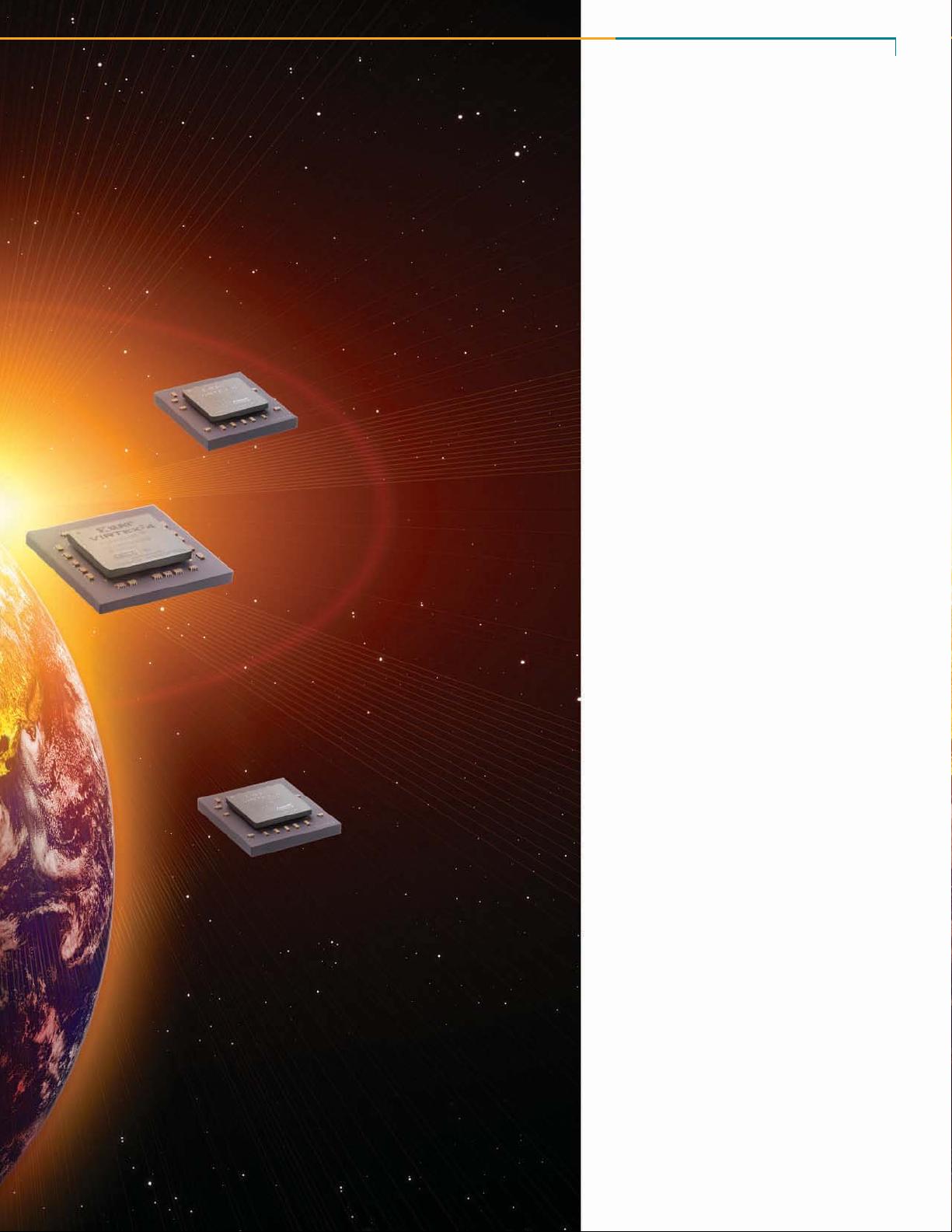
ation resistance in space-targeted designs.
Radiation-tolerant FPGAs such as the
14
Xcell Journal Third Quarter 2010
XCELLENCE IN AEROSPACE & DEFENSE
Rad-Hard FPGA Delivers State-of-the-Art Benefits
T
he Virtex-5QV offers a unique value proposition. This FPGA is rad-hard out of the box and also offers state-of-the-art
reprogrammable-logic density and hardwired IP blocks. Design teams working on space applications get ASIC-like
circuit density without the ASIC NRE costs.
The FPGA includes more than 130,000 logic cells for large, complex designs. The architecture is based on six-input LUTs
and the IC employs a diagonal interconnect structure that ultimately packs designs more efficiently in terms of silicon utiliza-
tion and results in better performance and lower power consumption.
The design is based on the second generation of Xilinx’s Advanced Silicon Modular Block (ASMBL™) column-based archi-
tecture. ASMBL has allowed Xilinx to produce mixes of configurable logic and hardwired IP that are optimized for specific
applications.
The Virtex-5QV includes 320 Enhanced DSP slices to complement the programmable logic. Each slice includes a 25 x 18-
bit multiplier, an adder and an accumulator. Designers can cascade the IC’s 36-kbit Block RAM elements to produce large, gen-
eral-purpose memory arrays. The device includes 298 such blocks. Each block can also be configured as two 18-kbit blocks, so
there is little wasted silicon for applications requiring smaller RAM arrays.
For networking and I/O operations, the Virtex-5QV includes a number of hardwired IP blocks. Six Ethernet media-access
controller (MAC) functions can operate in 10-, 100 and 1,000-Mbps modes. Eighteen RocketIO™ transceivers support data
transfers at rates ranging from 150 Mbps to 3.125 Gbps. The MACs can use some of the RocketI/O transceivers for physical-
layer (PHY) connections or link to external PHYs via a soft Media Independent Interface implemented in programmable logic.
The IC also includes three PCI Express
®
blocks compatible with the PCI Express Base Specification version 1.1. Designs can
implement x1-, x4- or x8-lane channels with each of the three blocks. The RocketIO transceivers are also available for PCI
Express I/O.
The device features a number of other functions important in high-performance system designs. Six clock management tiles
(CMTs) can each generate clocks that operate up to 450 MHz. Each CMT includes dual digital clock managers (DCMs) and
a phase-locked loop (PLL). The DCMs enable zero-delay buffering, frequency synthesis and clock-phase shifting. The PLLs add
support for input jitter filtering and phase-matched clock division.
Xilinx will manufacture the IC in a 65-nm copper CMOS process with a 1-V core voltage. A ceramic flip-chip column grid array
package will ensure signal integrity. And Xilinx will guarantee operation over the full military temperature range of -55ºC to +125ºC.
– Maury Wright


 我的内容管理
展开
我的内容管理
展开


