
Revision 3.0
March 2007
K1B6416B2D
- 4 -
UtRAM
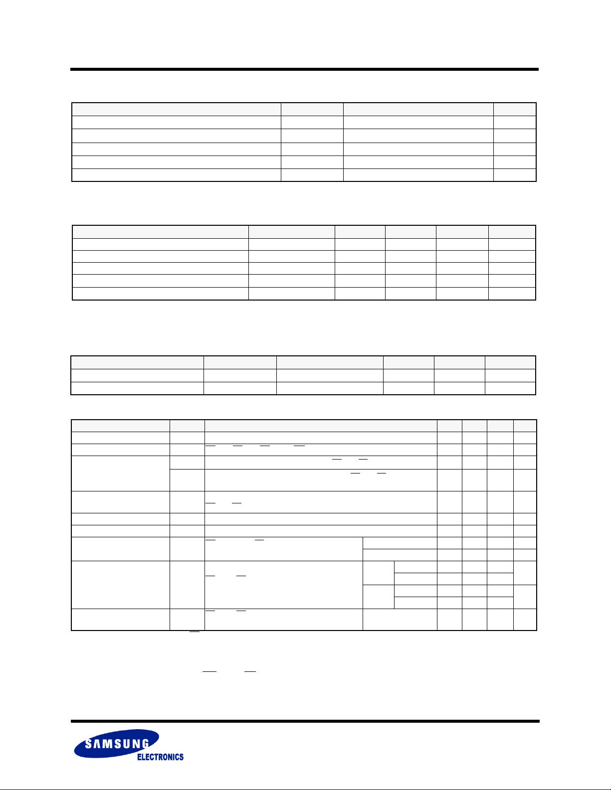
ABSOLUTE MAXIMUM RATINGS
1) Stresses greater than "Absolute Maximum Ratings" may cause permanent damage to the device. Functional operation should be restricted to be
used under recommended operating condition. Exposure to absolute maximum rating conditions longer than 1 second may affect reliability.
RECOMMENDED DC OPERATING CONDITIONS
1. TA=-40 to 85°C, otherwise specified.
2. Overshoot: V
CCQ +1.0V in case of pulse width ≤20ns. Overshoot is sampled, not 100% tested.
3. Undershoot: -1.0V in case of pulse width ≤20ns. Undershoot is sampled, not 100% tested.
CAPACITANCE (f=1MHz, TA=25°C)
DC AND OPERATING CHARACTERISTICS
1. ISB1 is measured after 60ms after CS high. CLK should be fixed at high or at Low.
2. Full Array Partial Refresh Current(I
SBP) is same as Standby Current(ISB1).
3. Internal TCSR (Temperature Compensated Self Refresh) is used to optimize refresh cycle below 40°C.
4. I
IO=0mA; This parameter is specified with the outputs disabled to avoid external loading effects.
5. V
IN=0V; all inputs should not be toggle.
6. Clock should not be inserted between ADV
low and WE low during Write operation.
Item Symbol Ratings Unit
Voltage on any pin relative to Vss
VIN, VOUT
-0.2 to VCCQ+0.3V V
Power supply voltage relative to Vss
VCC, VCCQ
-0.2 to 2.5V
V
Power Dissipation
PD
1.0 W
Storage temperature
TSTG
-65 to 150 °C
Operating Temperature
TA
-40 to 85 °C
Item Symbol Min Typ Max Unit
Power supply voltage(Core) VCC 1.7 1.8 1.95 V
Power supply voltage(I/O) V
CCQ 1.7 1.8 1.95 V
Ground V
SS, VSSQ 00 0V
Input high voltage
VIH
VCCQ-0.4 -
V
CCQ+0.2
2)
V
Input low voltage
VIL
-0.2
3)
-0.4V
Item Symbol Test Condition Min Max Unit
Input capacitance C
IN VIN=0V - 8 pF
Input/Output capacitance C
IO VIO=0V - 8 pF
Item Symbol Test Conditions Min Typ Max Unit
Input Leakage Current I
LI VIN=VSS to VCCQ -1 - 1 µA
Output Leakage Current I
LO CS=VIH, PS=VIH, OE=VIH or WE=VIL, VIO=Vss to VCCQ -1 - 1 µA
Average Operating
Current(Async)
I
CC2
Cycle time=70ns, IIO=0mA
4)
, 100% duty, CS=VIL, PS=VIH, VIN=VIL or VIH
--40mA
I
CC2P
Cycle time=tRC+3tPC, IIO=0mA
4)
, 100% duty, CS=VIL, PS=VIH, VIN=VIL or
V
IH
--40mA
Average Operating
Current(Sync)
I
CC3
Burst Length 4, Latency 5, 104MHz, IIO=0mA
4)
, Address transition 1 time,
CS
=VIL, PS=VIH, VIN=VIL or VIH
--40mA
Output Low Voltage V
OL IOL=0.2mA - - 0.2 V
Output High Voltage V
OH IOH=-0.2mA 1.4 - - V
Standby Current(CMOS)
I
SB1
1)
CS≥VCCQ-0.2V, PS≥VCCQ-0.2V, Other inputs=Vss
or V
CCQ (Toggle is not allowed)
5)
< 40°C - - 120 µA
< 85°C - - 180 µA
Partial Refresh Current
I
SBP
2)
PS≤0.2V, CS≥VCCQ-0.2V, Other inputs=Vss or
V
CCQ (Toggle is not allowed)
5)
< 40°C
1/2 Block - - 115
µA
1/4 Block - - 110
< 85°C
1/2 Block - - 165
µA
1/4 Block - - 155
Deep Power Down Current I
SBD
PS≤0.2V, CS≥VCCQ-0.2V, Other inputs=Vss or
VCCQ (Toggle is not allowed)
5)
< 85°C--30µA

剩余38页未读,继续阅读

�大师兄�
- 粉丝: 0
- 资源: 19
 我的内容管理
收起
我的内容管理
收起
- 我的资源
快来上传第一个资源
 我的收益 登录查看自己的收益
 我的积分
登录查看自己的积分
我的积分
登录查看自己的积分
 我的C币
登录后查看C币余额
我的C币
登录后查看C币余额
 我的收藏
我的收藏  我的下载
我的下载  下载帮助
下载帮助

会员权益专享


最新资源
- zigbee-cluster-library-specification
- JSBSim Reference Manual
- c++校园超市商品信息管理系统课程设计说明书(含源代码) (2).pdf
- 建筑供配电系统相关课件.pptx
- 企业管理规章制度及管理模式.doc
- vb打开摄像头.doc
- 云计算-可信计算中认证协议改进方案.pdf
- [详细完整版]单片机编程4.ppt
- c语言常用算法.pdf
- c++经典程序代码大全.pdf
- 单片机数字时钟资料.doc
- 11项目管理前沿1.0.pptx
- 基于ssm的“魅力”繁峙宣传网站的设计与实现论文.doc
- 智慧交通综合解决方案.pptx
- 建筑防潮设计-PowerPointPresentati.pptx
- SPC统计过程控制程序.pptx
资源上传下载、课程学习等过程中有任何疑问或建议,欢迎提出宝贵意见哦~我们会及时处理!
点击此处反馈


评论0