ELANSARY et al.: 50nW OPAMP-LESS -MODULATE D BIOIMPEDANCE SPECTRUM ANALYZER 1975
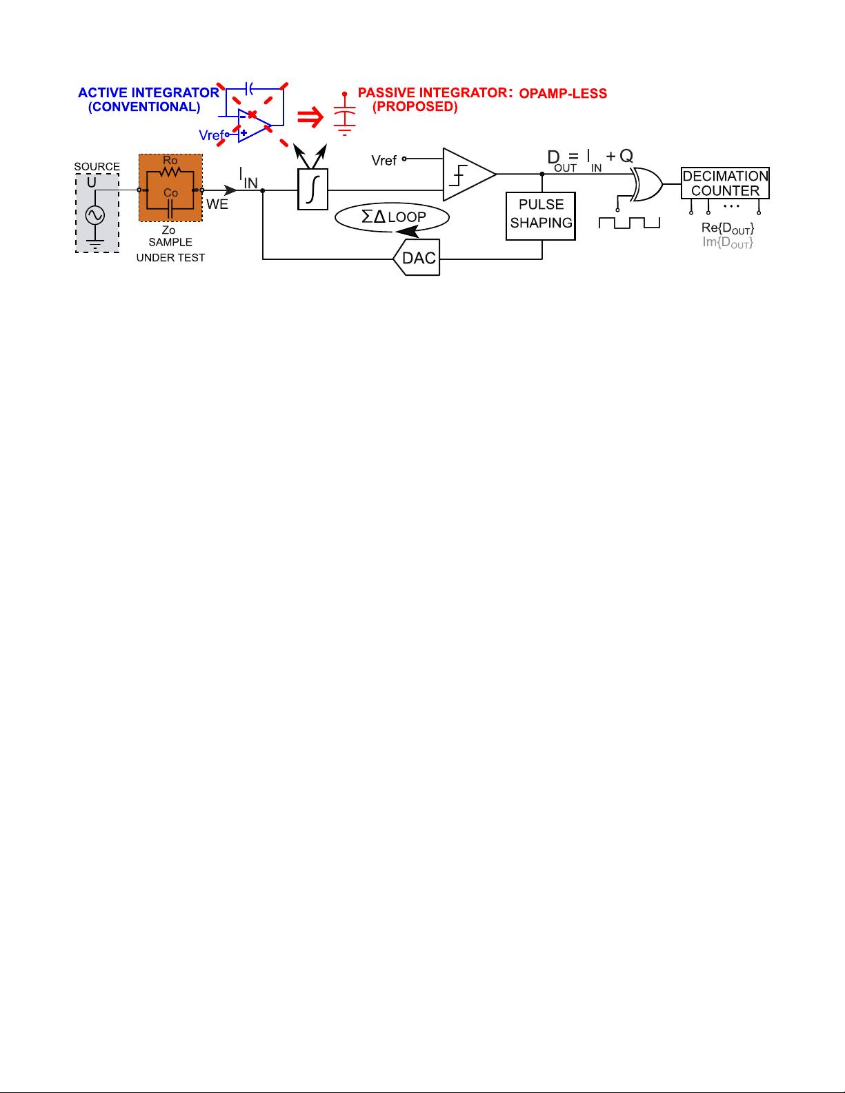
Fig. 5. Opamp-less -modulated ADC implementation: a conventional TIA integrator is replaced with a large capacitor as a passive integrator. The ADC
digital output is multiplied by a square wave using a simple
XOR gate.
higher frequencies and the quantization noise to be much lower
than Nyquist-rate ADCs at low frequencies (baseband). In the
proposed FRA scheme, the ADC output multibit multiplica-
tion by sinewave coefficients [Fig. 4(c) and (e)] is replaced
with a single-bit squarewave multiplication [Fig. 4(d) and (f)].
Replacing the high-resolution sinewave by its 1-bit squarewave
representatio n causes additional spectral components due to
the harmonics of the squarewave as shown in Fig. 4(f).
Due to the nature of the square wave, where the weight of
its harmonics decreases hyperbolically with frequency, the
strong high-frequency noise harmonics do not significantly
corrupt the outp ut result of the multiply-and-accumulate oper-
ation, allowing the system to take advantage of the low-noise
baseband, leading to a higher sensitivity when compared with
conventional implementations. Hence, the real and imaginary
components of Z are efficiently computed by using a single-bit
square wave, and a 90
◦
-delayed version of it, instead of
sin(ω
o
t) and cos(ω
o
t) f unctions. This eliminates th e need
to store these functions in a large and power-consuming
SRAM. Even more importantly, this also eliminates the area
and energy requirements of a multibit multiplier and adder,
which are prohibitive for implantable applications. In this case,
the reuse of a single MAC operation using time multiplexer
becomes unnecessarily co mplicated in this scheme, as simulta-
neous extraction of the real and imaginary components comes
with using only a single
XOR gate and a counter.
IV. O
PAMP-LESS ADC
The development of the biocompatible antifouling layer,
discussed in Section II, enables chronic implantation of the
proposed impedance spectrum analyzer. Chronic implantation
of biosensory devices is necessary for long-term studies, which
dictates specific requirements on the implanted device, such as
biocompatibility to avoid any tissue-implant reaction, small
form factor, high level of integration, and ultr alow power
consumption. While biocomatibility is taken care of by virtue
of the presented antifouling layer, low power consumption
and high integration level are ensured by the novel channel
architecture presented in this section.
For biochemical sensing, amperometry is required for mea-
suring ion concentrations. Typically, a transimpedance ampli-
fier (TIA) is employed to provide a minimal input impedance
and to maintain the input node voltage level unchanged
during current sensing. For these two requirements, a negative
feedback loop is necessary to set the virtual ground at the
input node of the readout circuit while providing the required
low input impedance. Conventionally, an amplifier (usually
an opamp/OTA) with a passive feedback network is used to
perform this function. To have the sufficient gain and band-
width for maintaining the feedback, 30% to 50% of the readout
circuitry power budget is consumed in the amplifier [4], [5],
[9], [16], whereas the rest of the power budget is divided
among ADC, digital signal processing, and biasing circuitry.
A major power reduction can be achieved if the negative
feedback is maintained without the use of an amplifier.
In the case of a delta-sigma ADC, an integrator is included
in the negative feedback loop to accumulate the loop
error and to produce an output bit stream that resembles
the analog input after decimation. In the presented channel,
we eliminate the opamp and replace the loop integrator by a
large capacitance C
INT
,inthewaydepictedinFig.5.This
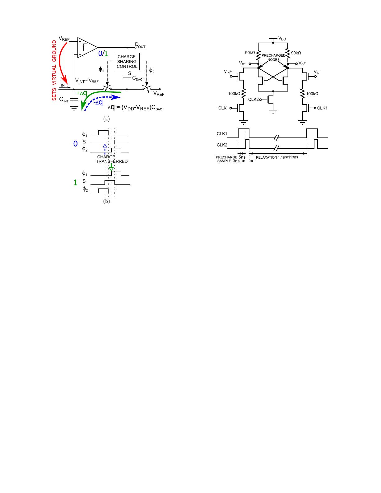
opamp-less negative feedback loop is used to maintain
a low input impedance and to set the virtual voltage at the
input node. The difference between the feedback and the input
currents is integrated on C
INT
, while the voltage at C
INT
,
which is also the input node, is set by the loop comparator
reference voltage V
REF
(Fig. 5). Since a capacitor has a very
high impedance at low frequencies, the feedback loop gain
is preserved for low-frequency input signals, which is well
suited for biomedical applications. Provided that the loop is
fast enough to track the voltage variations at the input node
(on C
INT
) caused by fast or relatively large input currents,
the operation of the loop is maintained and the input node
issetatV
REF
. This is achieved by choosing high sampling
frequency when compared with the input frequency as well as
other conditions that are detailed in Section IV-B.
In addition, as indicated in Sectio n III, the output stream
allows to perform the MAC operation inside the ADC itself
by replacing the multibit sin/cos multip lication with area- and
power-efficient single-b it squarewave multiplication [Fig. 4(b),
(d) and (f)].
A. Passive Integrators
As mentioned earlier in this section, a fundamental building
block in ADCs is the integrator (or the loop filter),
Authorized licensed use limited to: ShanghaiTech University. Downloaded on June 29,2020 at 14:06:42 UTC from IEEE Xplore. Restrictions apply.
