
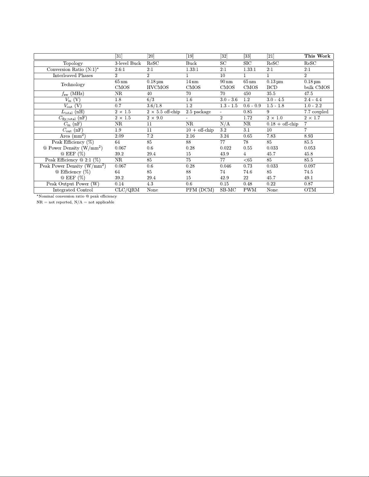
3182 IEEE JOURNAL OF SOLID-STATE CIRCUITS, VOL. 55, NO. 12, DECEMBER 2020
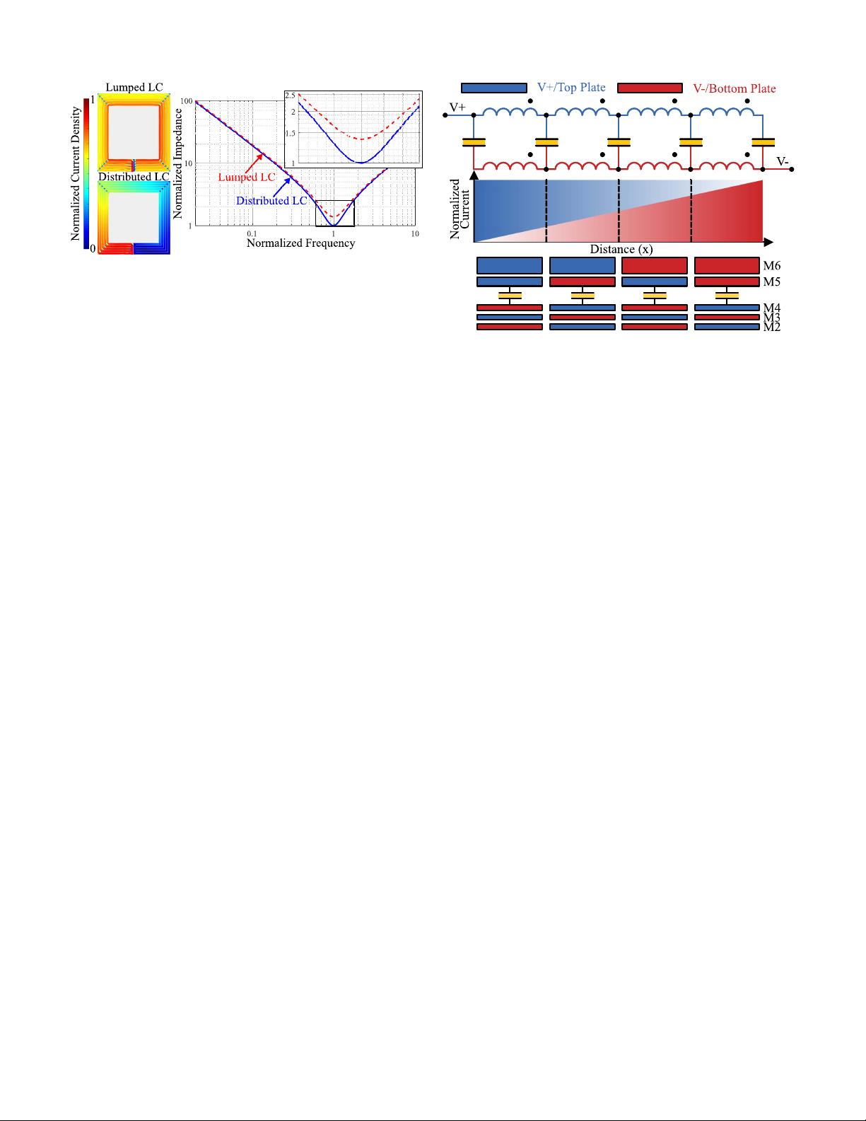
Fig. 7. Example EM simulation results for identical parallel trace spirals—
one with lumped capacitance and one with distributed capacitance—showing
current density plots and corresponding impedance magnitudes versus fre-
quency.
In Fig. 6(a), uniform trace widths are implemented and without
any ballasting mechanism the proximity effect dominates and
causes current to crowd to the innermost traces. In Fig. 6(b),
ballasting is accomplished by tuning both the width of each
parallel trace, and the capacitance distributed along its length,
resulting in uniform current density in each trace. In reality,
current will decrease in the top layer while increasing in the
bottom layer due to the distributed capacitance—an effect that
is seen in Fig. 7 and explained in Fig. 8—but the underlying
ballasting shown here is still present.
Considering the model shown in Fig. 6(b), current will
tend to flow relative to the admittance, Y
x
= Z
−1
x
, of each
trace. At low frequency (where capacitance dominates), if each
trace has matched capacitance (or capacitance per unit trace
width), then current would flow uniformly (or with uni-
form density). Such is the ballasting principle described and
implemented in [26]. Similarly, at high frequency, matching
the inductance would provide uniform current distribution.
However, at resonance (assuming each parallel trace has the
same resonant frequency), then as long as each trace has
the same resistance (or resistance per unit width), current
will be forced to flow uniformly (or with uniform density).
In practical implementations, magnetic coupling complicates
ballasting as the impedance of each trace depends to some
extent on its coupling to proximate traces. Regardless, the
goal of the ballasting procedure is to match the impedance
presented by each trace such that each has uniform current
density, which maximizes utilization of the available conductor
area, minimizing ESR, while maximizing Q.
In this effort, the design of the resonator shown in Fig. 5(b)
was completed with electromagnetic (EM) simulation and
tuning using Sonnet. Fig. 7 shows exemplary EM simulation
results of identical single-turn air-core spirals with lumped and
distributed capacitance (note that these are different from the
two-turn, coupled structure in Fig. 5, but illustrate a similar
benefit). From the current density plots, we can see that the
lumped version exhibits significant current crowding to the
inner conductors, while in the distributed LC resonator, cur-
rent is uniformly distributed across all traces. Both components
exhibit the same reactive impedances as seen at frequencies
above and below resonance, however the merged-LC structure
allows for full utilization of the available conductors. Thus, the
Fig. 8. Current density profile of capacitor plates versus distance in inductor
spiral and corresponding metal allocation.
two structures share the same resonant behavior, but improved
conductor utilization results in ∼40% lower ESR in this
example.
In addition to maximizing conductor utilization across the
horizontal cross section, the proposed structure also optimizes
allocation of metal layers in the vertical direction to minimize
conduction losses. Due to the embedded capacitance between
conductor layers, current density decreases in the top layer
with distance while increasing in the bottom layer. Assuming
the same dielectric constant at all locations in the spiral, the
current densities in each of the capacitor plates will follow
a linear profile and relative metal allocation can be scaled
accordingly.
Fig. 8 shows the impact of distributed capacitance along
the length of inductor windings on the current distribution
between capacitor plates. In an effort to trade off routing
complexity for performance enhancement, the total inductor
path length is split in four segments based on the current
profile shown. The metal allocation for each capacitor plate
is shown for each of the segments along with the single
MIM capacitance implemented in the merged-LC structure.
Metal M1 is left unused in order to minimize bottom plate
capacitance and metals M5 and M6 are two and six times as
thick as the underlying metals, respectively. The implemented
stackup results in a ∼29% reduction in conduction losses when
compared to a design with uniform metal allocation over the
length of the spiral.
As mentioned in the introduction, a final but important
benefit of the ReSC architecture is the reduction of eddy-
current losses in the substrate. Compared to a conventional
buck converter, the resonant architecture achieves favorable
tradeoffs between the magnitude (and spectral content) of the
inductor current ripple and the switching frequency. With a
buck converter, the current ripple is a function of switching fre-
quency, input voltage, and inductance (i.e., I ∝ V
in
/ f
sw
L),
and is a relatively high spectral content “ramp” waveform.
In a ReSC converter, flying capacitors effectively decouple
the sinusoidal inductor current ripple from input voltage,
such that it is only a function of load current; this enables
Authorized licensed use limited to: Xian Jiaotong University. Downloaded on November 25,2020 at 13:19:56 UTC from IEEE Xplore. Restrictions apply.
剩余296页未读,继续阅读

netshell
- 粉丝: 11
- 资源: 185
 我的内容管理
展开
我的内容管理
展开


最新资源
- 计算机人脸表情动画技术发展综述
- 关系数据库的关键字搜索技术综述:模型、架构与未来趋势
- 迭代自适应逆滤波在语音情感识别中的应用
- 概念知识树在旅游领域智能分析中的应用
- 构建is-a层次与OWL本体集成:理论与算法
- 基于语义元的相似度计算方法研究:改进与有效性验证
- 网格梯度多密度聚类算法:去噪与高效聚类
- 网格服务工作流动态调度算法PGSWA研究
- 突发事件连锁反应网络模型与应急预警分析
- BA网络上的病毒营销与网站推广仿真研究
- 离散HSMM故障预测模型:有效提升系统状态预测
- 煤矿安全评价:信息融合与可拓理论的应用
- 多维度Petri网工作流模型MD_WFN:统一建模与应用研究
- 面向过程追踪的知识安全描述方法
- 基于收益的软件过程资源调度优化策略
- 多核环境下基于数据流Java的Web服务器优化实现提升性能
资源上传下载、课程学习等过程中有任何疑问或建议,欢迎提出宝贵意见哦~我们会及时处理!
点击此处反馈


