16
The two wire serial bus interface
is used to allow an external micro
other information from the internal registers. MC_SCLK is the serial clock and MC_SDA is the data line. Both lines are
pulled high by resistors connected to VDD. I
open drain outputs. In normal operation the master generates all clock pulses, but control of the MC_SDA line alternates
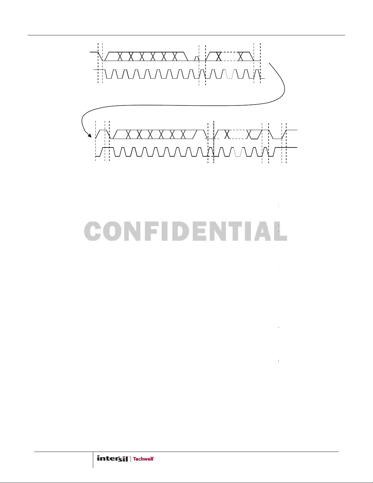
back and forth between the master and the slave. For both read and write, each byte is transferred MSB first, and the
data bit is valid whenever MC_SCLK is high.
The device is operated as a bus slave device
control bit to form the first byte transferred during a new transfer. If the read/write
a
read from the slave device. If it is low the next byte will be a write to the slave. When a bus master (the host
microprocessor) drives MC_SDA from high to low, while MC_SCLK is high, this is defined to be a sta
Figure 1
). All slaves on the bus listen to determine when a start condition has been asserted.
After a start condition, all slave
devices listen for their device addresses. The host then sends a byte consisting of the 7
bit slave device ID and the R/W bit. This is shown in
and is a write to the device therefore the first R/W bit is normally low.)
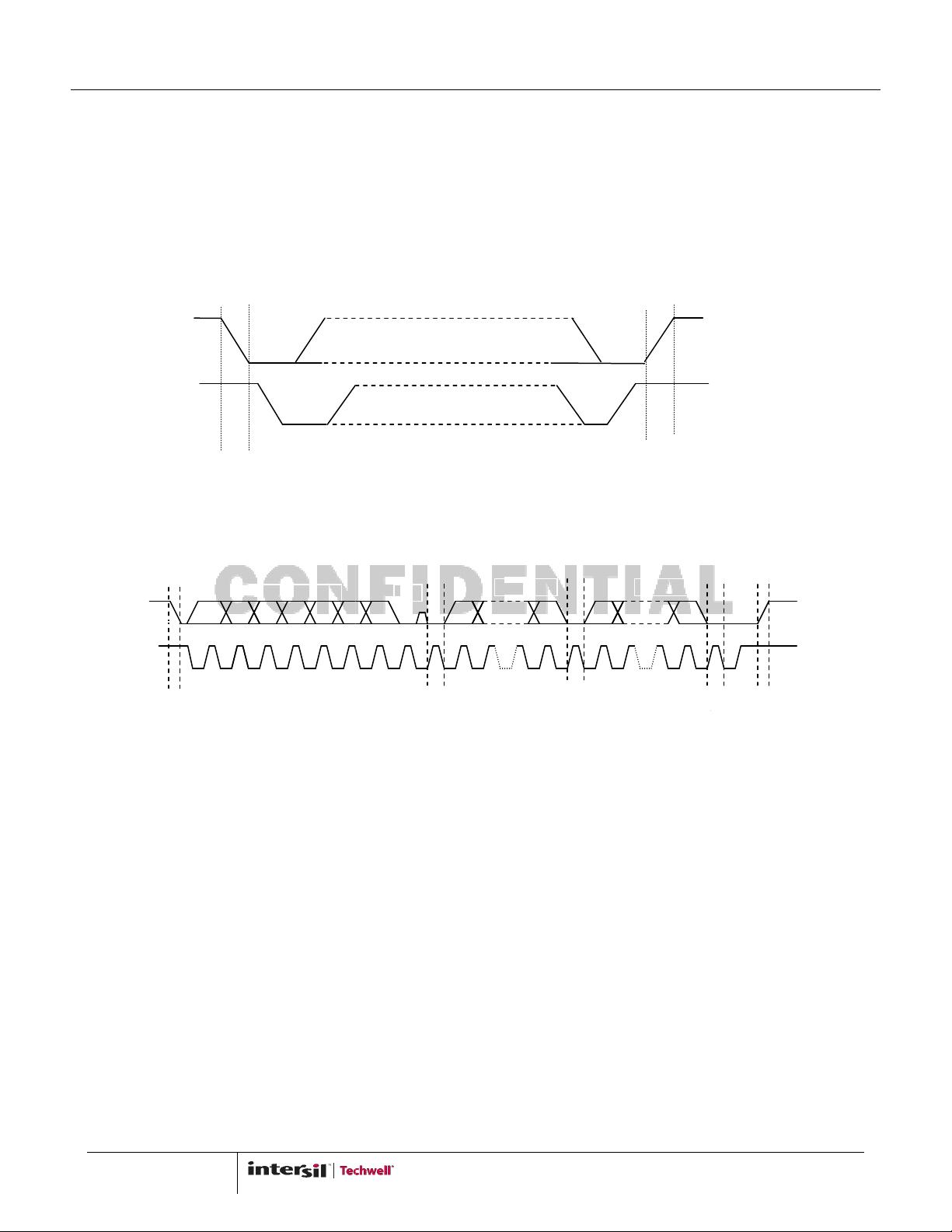
After transmitting the device address and the R/W bit, the master must release the MC_SDA line while holding MC_SC
low, and wait for an acknowledgement from the slave. If the address matches the device address of a slave, the slave
will respond by driving the MC_SDA line low to acknowledge the condition. The master will then continue with the next 8
bit transfer. If
no device on the bus responds, the master transmits a stop condition and ends the cycle. Notice that a
successful transfer always includes nine clock pulses.
To write to the internal register, the master sends another 8
internal index register. The device will acknowledge the 8
preparation for the next data. The master can do multiple writes if they are in ascending sequential order. Afte
bit transfer the device will acknowledge the receipt of the 8
host has to issue a stop condition.
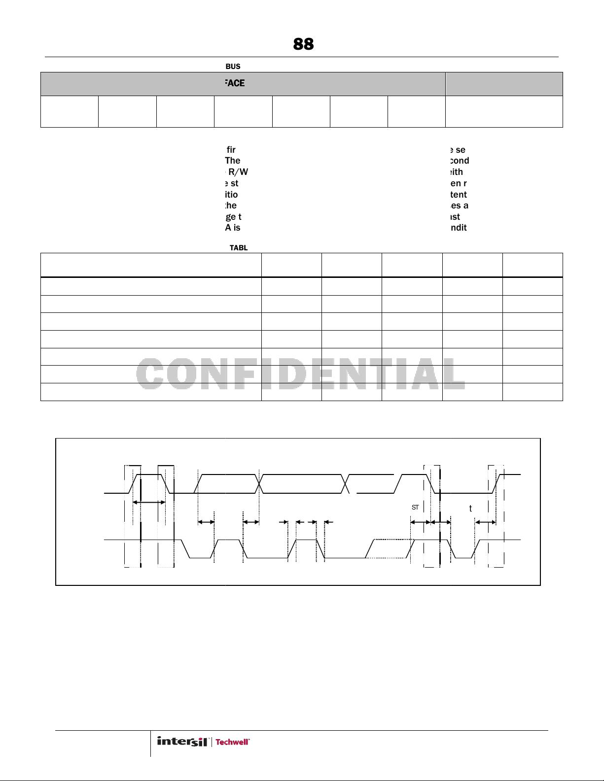
Condition
MC_SCLK
Condition
FIGURE 3.
TW8819
is used to allow an external micro
-controller to
write control data to, and read control or
other information from the internal registers. MC_SCLK is the serial clock and MC_SDA is the data line. Both lines are
pulled high by resistors connected to VDD. I
C
s communicate on the bus by pulling MC_SCLK and M
open drain outputs. In normal operation the master generates all clock pulses, but control of the MC_SDA line alternates
back and forth between the master and the slave. For both read and write, each byte is transferred MSB first, and the
data bit is valid whenever MC_SCLK is high.
The device is operated as a bus slave device
. The 7-bit device address field is fixed and
concatenated with the read/write
control bit to form the first byte transferred during a new transfer. If the read/write
control bit is high the next byte will be
read from the slave device. If it is low the next byte will be a write to the slave. When a bus master (the host
microprocessor) drives MC_SDA from high to low, while MC_SCLK is high, this is defined to be a sta
). All slaves on the bus listen to determine when a start condition has been asserted.
devices listen for their device addresses. The host then sends a byte consisting of the 7
bit slave device ID and the R/W bit. This is shown in
Figure 2
. (The next byte is normally the index to the internal registers
and is a write to the device therefore the first R/W bit is normally low.)
After transmitting the device address and the R/W bit, the master must release the MC_SDA line while holding MC_SC
low, and wait for an acknowledgement from the slave. If the address matches the device address of a slave, the slave
will respond by driving the MC_SDA line low to acknowledge the condition. The master will then continue with the next 8
no device on the bus responds, the master transmits a stop condition and ends the cycle. Notice that a
successful transfer always includes nine clock pulses.
To write to the internal register, the master sends another 8
-bits of data, it loads this to th
e register pointed by the
internal index register. The device will acknowledge the 8
-
bit data transfer and automatically increment the index in
preparation for the next data. The master can do multiple writes if they are in ascending sequential order. Afte
bit transfer the device will acknowledge the receipt of the 8
-
bits with an acknowledgement pulse. To end all transfers, the
Nack
Ack
R READ SEQUENCE VIA THE SERIAL BUS INTER
write control data to, and read control or
other information from the internal registers. MC_SCLK is the serial clock and MC_SDA is the data line. Both lines are
s communicate on the bus by pulling MC_SCLK and M
C_SDA low through
open drain outputs. In normal operation the master generates all clock pulses, but control of the MC_SDA line alternates
back and forth between the master and the slave. For both read and write, each byte is transferred MSB first, and the
concatenated with the read/write
control bit is high the next byte will be
read from the slave device. If it is low the next byte will be a write to the slave. When a bus master (the host
microprocessor) drives MC_SDA from high to low, while MC_SCLK is high, this is defined to be a sta
rt condition (see
devices listen for their device addresses. The host then sends a byte consisting of the 7
-
. (The next byte is normally the index to the internal registers
After transmitting the device address and the R/W bit, the master must release the MC_SDA line while holding MC_SC
LK
low, and wait for an acknowledgement from the slave. If the address matches the device address of a slave, the slave
will respond by driving the MC_SDA line low to acknowledge the condition. The master will then continue with the next 8
-
no device on the bus responds, the master transmits a stop condition and ends the cycle. Notice that a
e register pointed by the
bit data transfer and automatically increment the index in
preparation for the next data. The master can do multiple writes if they are in ascending sequential order. Afte
r each 8-
bits with an acknowledgement pulse. To end all transfers, the
Condition

 我的内容管理
展开
我的内容管理
展开


