TS3USB221E:高速USB2.0信号1:2多路复用/分离器
需积分: 9 59 浏览量
更新于2024-06-28
4
收藏 2.1MB PDF 举报
"TI-TS3USB221E.pdf 是一款由德州仪器(TI)生产的高速USB2.0 1:2多路复用器/分离器,具有单使能端口和IEC3级ESD保护功能。"
TS3USB221E是一款高性能的集成电路,设计用于高速USB2.0数据传输,支持480Mbps的速率。这款器件的主要特点包括:
1. **电源电压范围**:TS3USB221E可在2.3V至3.6V的电压范围内工作,这使其适用于多种电压环境下的系统。
2. **开关I/O耐压能力**:它能够处理高达5.5V的信号,提供了对较高电压信号的兼容性。
3. **控制引脚兼容性**:控制引脚输入兼容1.8V,这使得它可以在低电压系统中操作。
4. **低功耗模式**:当OE(Output Enable)禁用时,器件进入低功耗模式,电流消耗仅为1μA,有助于降低整体系统功耗。
5. **开关性能**:具有低导通电阻(rON)为6Ω的最大值,以及极小的导通电阻差(ΔrON)为0.2Ω的典型值,确保了信号传输的高效和低损耗。
6. **电容负载**:Cio(on)的最大值为7pF,这有助于减少信号衰减。
7. **ESD保护**:按照JESD22标准进行测试,能承受7000V人体放电模型和1000V充电器件模型。此外,I/O端口还具备ESD接地保护,包括12kV人体放电模型和±7kV接触放电(IEC61000-4-2)。
8. **高带宽**:器件的带宽高达1GHz,保证了高速USB信号的高质量传输,减少信号失真。
9. **应用领域**:适用于各种设备,如USB1.0、1.1和2.0的信号路由,手机,数码相机,笔记本电脑,USBI/O扩展以及MHL1.0等。
这款开关专为那些USB I/O接口受限的便携式设备设计,如手机和数码相机,它能够有效地管理和切换高速USB2.0信号,确保数据传输的稳定性和可靠性。通过其优秀的ESD保护特性,TS3USB221E能够在各种环境条件下提供保护,延长设备的使用寿命。在实际设计中,应参考最新的英文版数据手册以获取最准确的技术信息。
6
TS3USB221E
ZHCSK77D –SEPTEMBER 2009–REVISED SEPTEMBER 2019
www.ti.com.cn
Copyright © 2009–2019, Texas Instruments Incorporated
(1) For Maximum or Minimum conditions, use the appropriate value specified under Electrical Characteristics for the applicable device type.
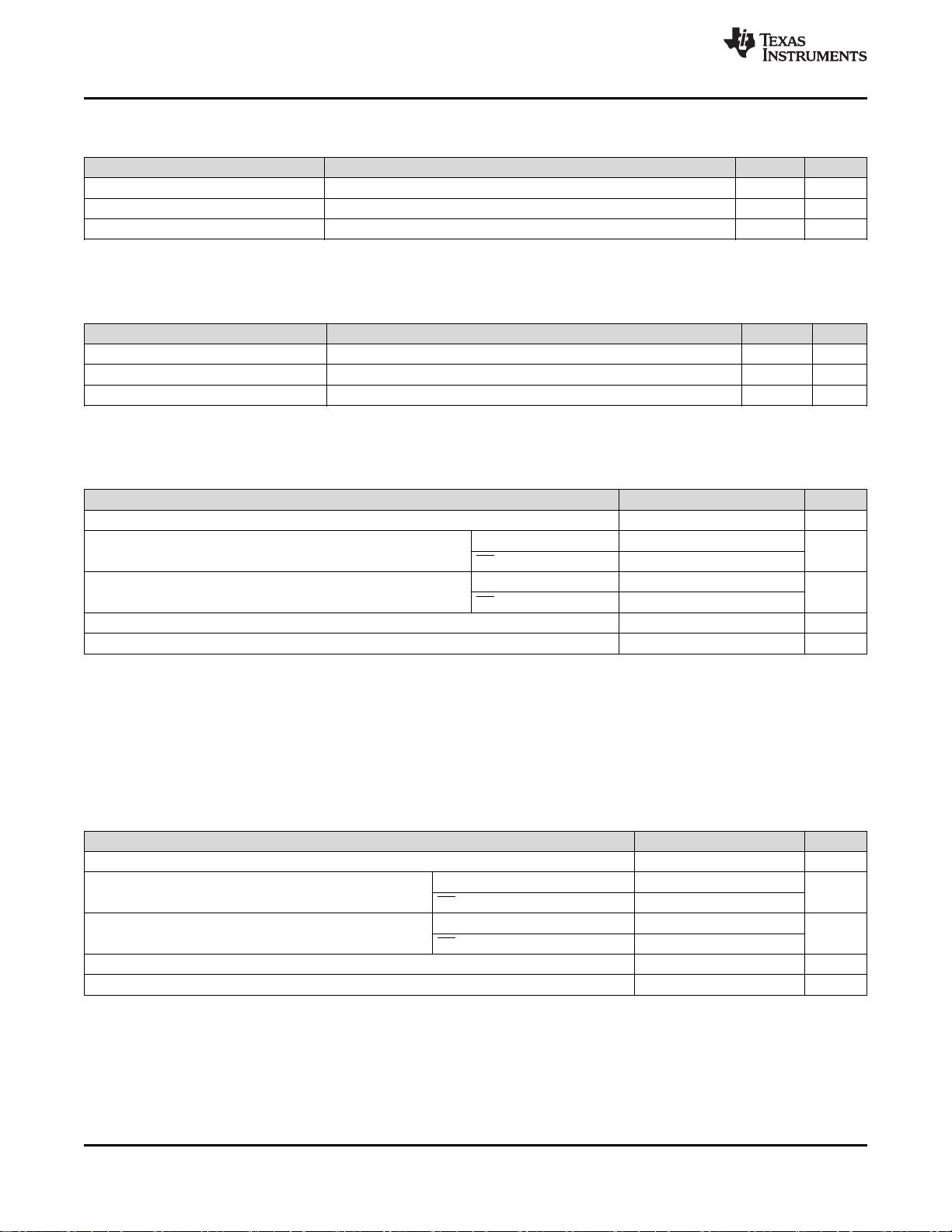
6.6 Dynamic Electrical Characteristics, V
CC
= 3.3 V ±10%
over operating range, T
A
= –40°C to 85°C, V
CC
= 3.3 V ±10%, GND = 0 V
PARAMETER TEST CONDITIONS TYP
(1)
UNIT
X
TALK
Crosstalk R
L
= 50 , f = 250 MHz –40 dB
O
IRR
OFF isolation R
L
= 50 , f = 250 MHz –40 dB
BW Bandwidth (–3 dB) R
L
= 50 1 GHz
(1) For Maximum or Minimum conditions, use the appropriate value specified under Electrical Characteristics for the applicable device type.
6.7 Dynamic Electrical Characteristics, V
CC
= 2.5 V ±10%
over operating range, T
A
= –40°C to 85°C, V
CC
= 2.5 V ±10%, GND = 0 V
PARAMETER TEST CONDITIONS TYP
(1)
UNIT
X
TALK
Crosstalk R
L
= 50 , f = 250 MHz -39 dB
O
IRR
OFF isolation R
L
= 50 , f = 250 MHz -40 dB
BW Bandwidth (3 dB) R
L
= 50 1 GHz
(1) For Maximum or Minimum conditions, use the appropriate value specified under Electrical Characteristics for the applicable device type.
(2) Specified by design
(3) The bus switch contributes no propagational delay other than the RC delay of the on resistance of the switch and the load capacitance.
The time constant for the switch alone is of the order of 0.25 ns for 10-pF load. Because this time constant is much smaller than the
rise/fall times of typical driving signals, it adds very little propagational delay to the system. Propagational delay of the bus switch, when
used in a system, is determined by the driving circuit on the driving side of the switch and its interactions with the load on the driven
side.
6.8 Switching Characteristics, V
CC
= 3.3 V ±10%
over operating range, T
A
= –40°C to 85°C, V
CC
= 3.3 V ±10%, GND = 0 V
PARAMETER MIN TYP
(1)
MAX UNIT
t
pd
Propagation delay
(2) (3)
0.25 ns
t
ON
Line enable time
S to D, nD 30
ns
OE to D, nD 17
t
OFF
Line disable time
S to D, nD 12
ns
OE to D, nD 10
t
SK(O)
Output skew between center port to any other port
(2)
0.1 0.2 ns
t
SK(P)
Skew between opposite transitions of the same output (t
PHL
– t
PLH
)
(2)
0.1 0.2 ns
(1) For Maximum or Minimum conditions, use the appropriate value specified under Electrical Characteristics for the applicable device type.
(2) Specified by design
(3) The bus switch contributes no propagational delay other than the RC delay of the on resistance of the switch and the load capacitance.
The time constant for the switch alone is of the order of 0.25 ns for 10-pF load. Because this time constant is much smaller than the
rise/fall times of typical driving signals, it adds very little propagational delay to the system. Propagational delay of the bus switch, when
used in a system, is determined by the driving circuit on the driving side of the switch and its interactions with the load on the driven
side.
6.9 Switching Characteristics, V
CC
= 2.5 V ±10%
over operating range, T
A
= –40°C to 85°C, V
CC
= 2.5 V ±10%, GND = 0 V
PARAMETER MIN TYP
(1)
MAX UNIT
t
pd
Propagation delay
(2) (3)
0.25 ns
t
ON
Line enable time
S to D, nD 50
ns
OE to D, nD 32
t
OFF
Line disable time
S to D, nD 23
ns
OE to D, nD 12
t
SK(O)
Output skew between center port to any other port
(2)
0.1 0.2 ns
t
SK(P)
Skew between opposite transitions of the same output (t
PHL
– t
PLH
)
(2)
0.1 0.2 ns
剩余29页未读,继续阅读
点击了解资源详情
点击了解资源详情
点击了解资源详情
2022-12-01 上传
2022-12-01 上传
2022-12-01 上传
2022-12-01 上传
2022-12-03 上传
2022-12-03 上传

不觉明了
- 粉丝: 4228
- 资源: 5759
 我的内容管理
展开
我的内容管理
展开


最新资源
- 深入浅出:自定义 Grunt 任务的实践指南
- 网络物理突变工具的多点路径规划实现与分析
- multifeed: 实现多作者间的超核心共享与同步技术
- C++商品交易系统实习项目详细要求
- macOS系统Python模块whl包安装教程
- 掌握fullstackJS:构建React框架与快速开发应用
- React-Purify: 实现React组件纯净方法的工具介绍
- deck.js:构建现代HTML演示的JavaScript库
- nunn:现代C++17实现的机器学习库开源项目
- Python安装包 Acquisition-4.12-cp35-cp35m-win_amd64.whl.zip 使用说明
- Amaranthus-tuberculatus基因组分析脚本集
- Ubuntu 12.04下Realtek RTL8821AE驱动的向后移植指南
- 掌握Jest环境下的最新jsdom功能
- CAGI Toolkit:开源Asterisk PBX的AGI应用开发
- MyDropDemo: 体验QGraphicsView的拖放功能
- 远程FPGA平台上的Quartus II17.1 LCD色块闪烁现象解析
