The "Microcomputer Principles and Applications: Chapter 2 8086 System Architecture" and "Microcomputer Principles and Applications: Chapter 2 8086 System Architecture" cover the following topics:
2.1 8086/8088 CPU Internal Structure
2.2 8086/8088 CPU Pins and Functions
2.3 8086/8088 System Organization
2.4 8086/8088 CPU Timing
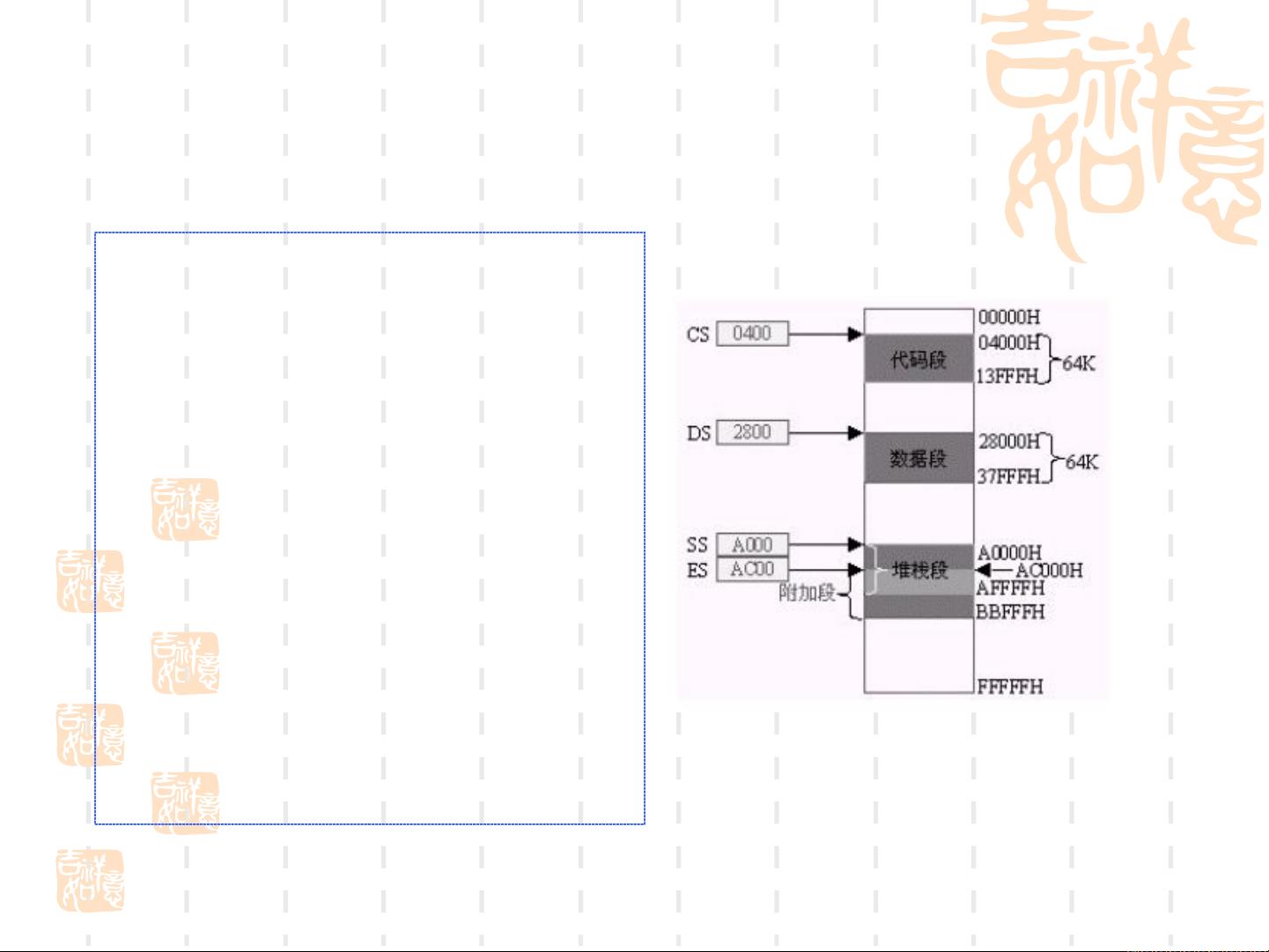
The 8086/8088 CPU internal structure is made up of two independent processing units. The Execution Unit (EU) comprises 8 16-bit registers, including general-purpose registers AX, BX, CX, and DX; index registers SP and BP; and offset registers SI and DI. The EU also includes an Arithmetic Logic Unit (ALU), Flag Register (FR), and temporary registers, as well as the EU control system. The Bus Interface Unit (BIU) includes four segment registers CS, SS, DS, and ES.
The CPU structure and characteristics are explained in detail, emphasizing the independence of the processing units and the specific functions of each unit. The EU and BIU work together to execute instructions and manage the flow of data within the CPU.
Additionally, the CPU pins and functions are described, detailing the role of each pin and its contribution to the overall functionality of the CPU. The system organization of the 8086/8088 CPU is also outlined, illustrating how the different components work together to process and execute instructions.
The CPU timing is a critical aspect of the 8086/8088 CPU, as it determines the speed and efficiency of the processing unit. The timing is carefully managed to ensure the accurate execution of instructions and the synchronization of the different components within the CPU.
Overall, the 8086/8088 CPU is a complex and sophisticated processing unit with a well-defined internal structure, detailed pin functions, and carefully managed system organization and timing. Understanding these key aspects is essential for effectively utilizing and programming the 8086/8088 CPU in various applications.