
CoolSET™ F3R80
ICE3AR1080VJZ
Pin Configuration and Functionality
Data Sheet 8 V2.0, 2014-01-20
1 Pin Configuration and Functionality
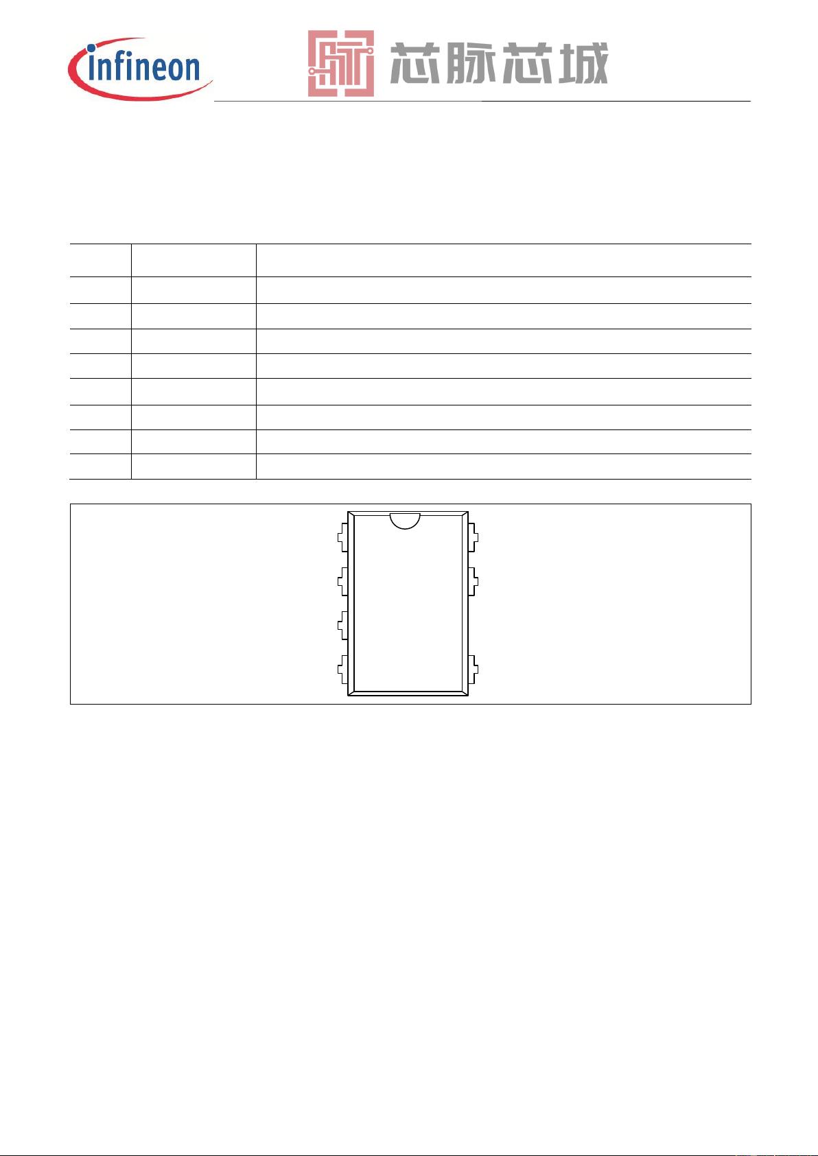
1.1 Pin Configuration with PG-DIP-7
Pin
Symbol
Function
1
BV
extended Blanking time & input OVP
2
FBB
Feedback & Burst entry/exit control
3
CS
Current Sense/ 800V CoolMOS™ Source
4
n.c.
not connected
5
Drain
800V CoolMOS™ Drain
6
-
(no pin)
7
VCC
Controller Supply Voltage
8
GND
Controller Ground
1
7
8
4
3
2
5
GNDBV
FBB
CS
VCC
n.c. Drain
Figure 2: Pin configuration PG-DIP-7(top view)
1.2 Pin Functionality
BV (extended Blanking time & input OVP)
The BV pin combines the functions of input OVP and extendable blanking time for over load protection. The input
OVP feature is to stop the switching pulse when the input line voltage is higher than the V
OVP_ref
after the resistor
divider (Refer to Figure 3). The extendable blanking time function is to extend the built-in 20 ms blanking time for
over load protection by adding an external capacitor to ground.
FBB (Feedback & Burst entry control)
The FBB pin combines the feedback function and the burst entry/exit control. The regulation information is
provided by the FBB pin to the internal Protection Unit and the internal PWM-Comparator to control the duty cycle.
The FBB-signal is the only control signal in case of light load at the Active Burst Mode. The burst entry/ exit control
provides an access to select the entry/exit burst mode level.
CS (Current Sense)
The Current Sense pin senses the voltage developed on the shunt resistor inserted in the source of the integrated
CoolMOS™. If CS reaches the internal threshold of the Current Limit Comparator, the Driver output is immediately
switched off. Furthermore the current information is provided for the PWM comparator to realize the Current Mode.

剩余42页未读,继续阅读

芯脉芯城
- 粉丝: 3
- 资源: 4030
 我的内容管理
收起
我的内容管理
收起
- 我的资源
快来上传第一个资源
 我的收益 登录查看自己的收益
 我的积分
登录查看自己的积分
我的积分
登录查看自己的积分
 我的C币
登录后查看C币余额
我的C币
登录后查看C币余额
 我的收藏
我的收藏  我的下载
我的下载  下载帮助
下载帮助

会员权益专享


最新资源
- 电力电子系统建模与控制入门
- SQL数据库基础入门:发展历程与关键概念
- DC/DC变换器动态建模与控制方法解析
- 市***专有云IaaS服务:云主机与数据库解决方案
- 紫鸟数据魔方:跨境电商选品神器,助力爆款打造
- 电力电子技术:DC-DC变换器动态模型与控制
- 视觉与实用并重:跨境电商产品开发的六重价值策略
- VB.NET三层架构下的数据库应用程序开发
- 跨境电商产品开发:关键词策略与用户痛点挖掘
- VC-MFC数据库编程技巧与实现
- 亚马逊新品开发策略:选品与市场研究
- 数据库基础知识:从数据到Visual FoxPro应用
- 计算机专业实习经验与项目总结
- Sparkle家族轻量级加密与哈希:提升IoT设备数据安全性
- SQL数据库期末考试精选题与答案解析
- H3C规模数据融合:技术探讨与应用案例解析
资源上传下载、课程学习等过程中有任何疑问或建议,欢迎提出宝贵意见哦~我们会及时处理!
点击此处反馈


