272 IEEE JOURNAL OF SOLID-STATE CIRCUITS, VOL. 56, NO. 1, JANUARY 2021
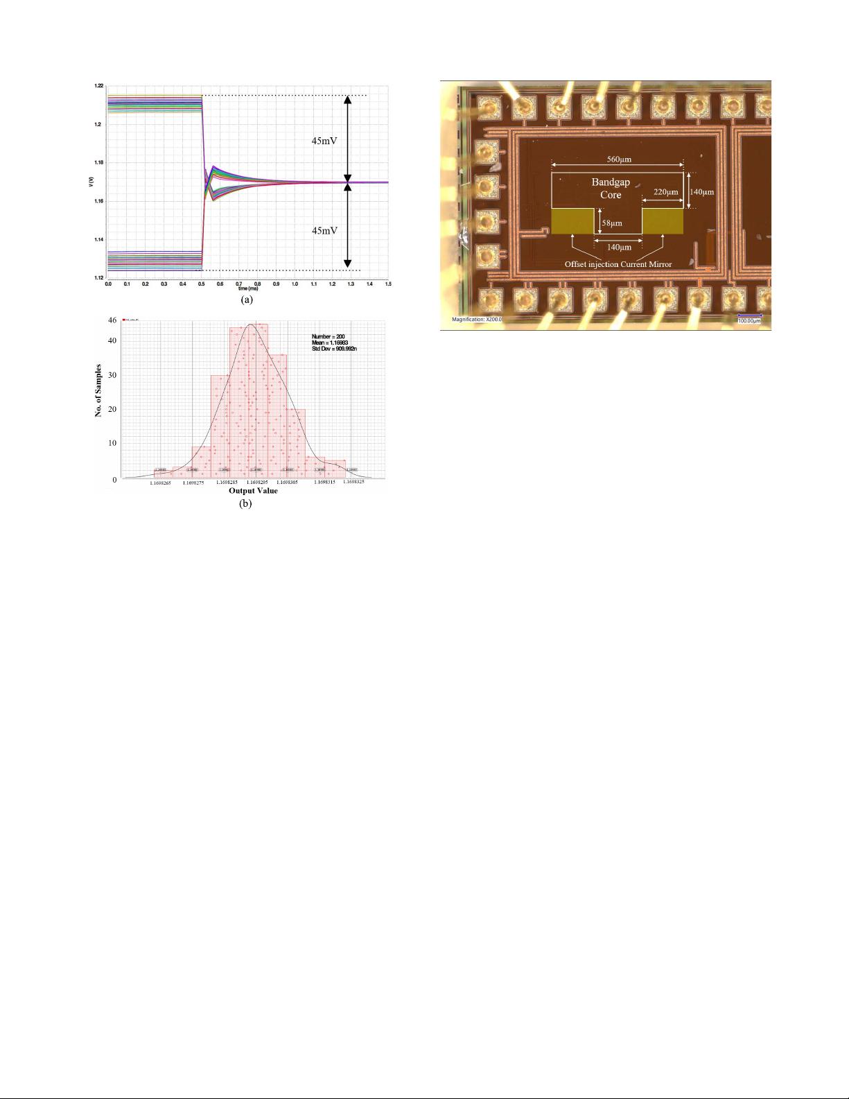
Fig. 6. (a) Simulated bandgap output v oltages with injected offset currents
to induce positive/negative output deviations before/after the acti vation of
the automatic offset cancellation. (b) Monte Carlo simulation results for the
bandgap output voltage (without the impact of BJT and resistor mismatches).
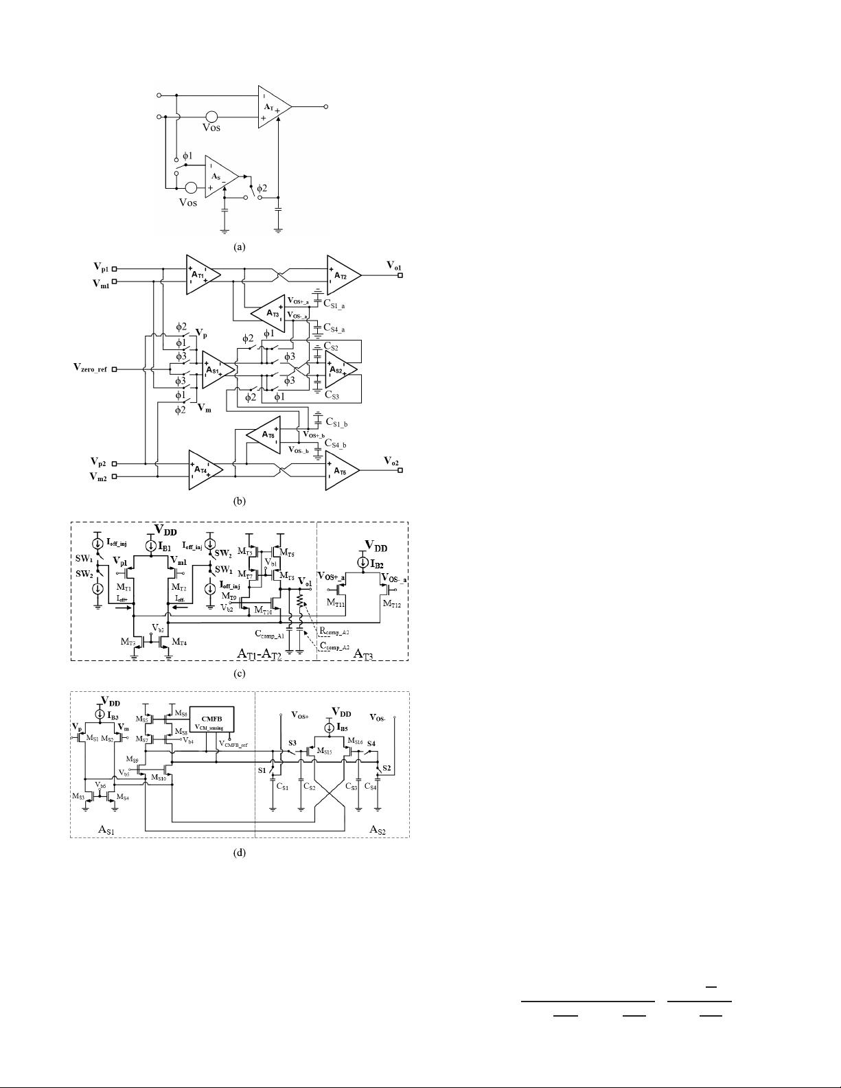
stored on C
s2
and C
s3
when the circuit is in the amplification
mode. To ensure continuous operation of the main amplifiers,
the capacitors C
s1
and C
s4
are utilized to store the offset-
cancellation information for both amplifiers under calibration
(during their respective phases φ1andφ2) when the circuit
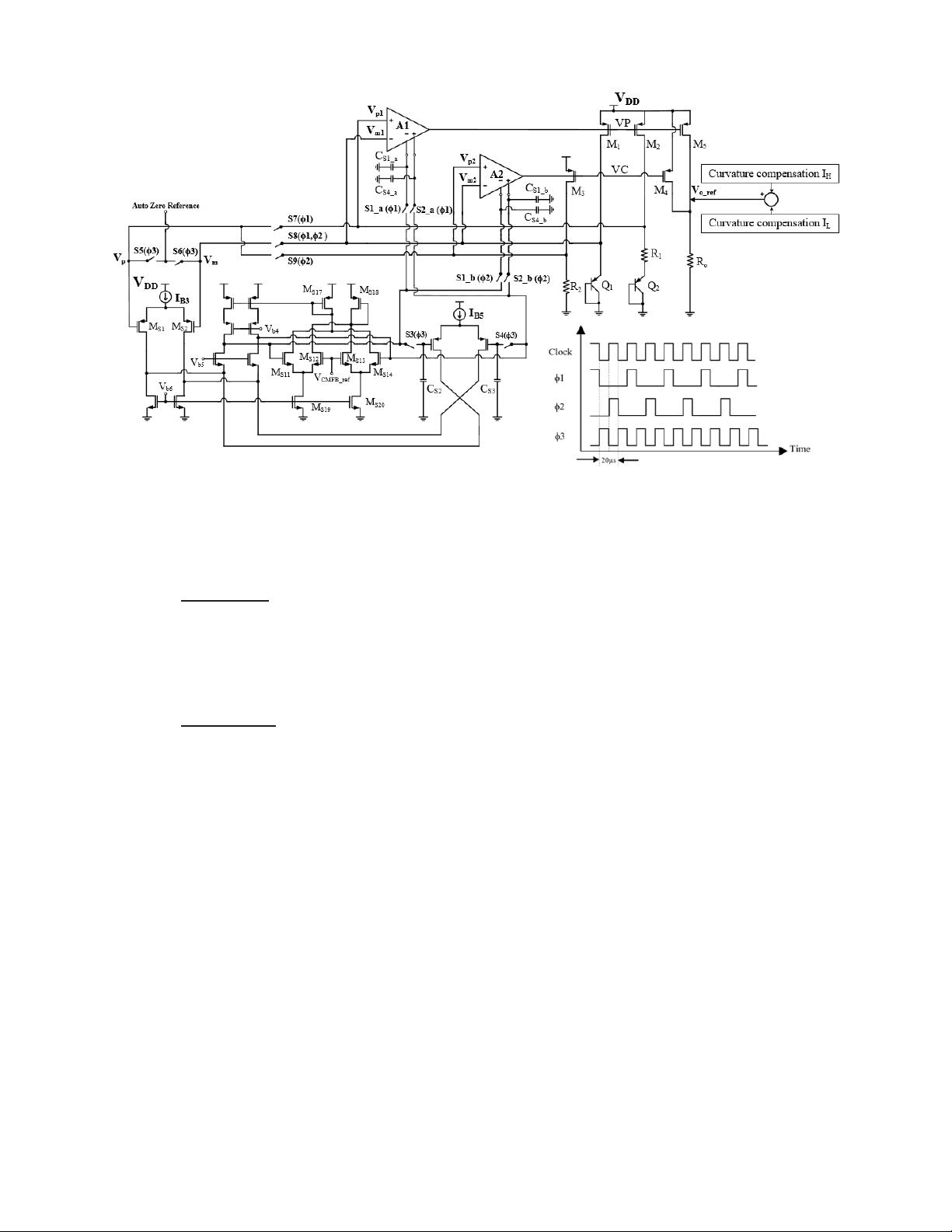
is in the auto-zero phase. The curvature compensation circuit
from Fig. 2 (c) is connected to the output of the b andgap
circuit to provide multi-sectional compensation.
III. E
XPERIMENTAL RESULTS
To evaluate the performance of the offset-cancellation tech-
nique, several current mirrors were included in the main
amplifiers of the bandgap reference to inject currents [I
off_inj
in Fig. 4(c)] to purposely generate variable imbalances (i.e.,
amplifier offset voltages) with external control. Since the offset
voltage of an amplifier also has some temperature depen-
dence, the manually introduced offset range should cover the
worst case offset voltage. During the simulations, the injected
offset current emulates the worst case input-referred offset
condition for both amplifiers. Furthermore, the active offset
compensation alleviates the temperature dependence due to
its continuous operation in the background.
Fig. 6(a) shows transient simulation results of the bandgap
reference circuit obtained with process corner models for
the devices. Prior to the activation of the offset-cancellation
circuits at 500 μs, the worst case shift of the bandgap
reference output voltage is ±45 mV. After activation of the
Fig. 7. Die photograph of proposed bandgap reference circuit design.
offset-cancellation circuitry, this o utput voltage error reduces
to ±100 μV within 125 μs. Monte Carlo simulations were
completed using foundry-supplied statistical device models
with mismatch and process variations activated. Since the
differential pair is laid out with matching techniques, a cor-
relation coefficient of 0.95 was specified for the m atched
devices [20]. Fig. 6(b) d isplays the results from 200 Monte
Carlo runs, showing that the estimated bandgap voltage stan-
dard deviation is 0.91 μV with the offset cancellation; here,
in order to evaluate the performance of the active offset-
cancellation circuit, mismatch on the transistors inside both
the amplifier under calibration and the auxiliary amplifier
is enabled. The mismatches among the r esistors and BJTs
were not included in this Monte Carlo simulation since the
circuit cannot reduce the output voltage shift caused by these
non-idealities.
The die photograph is shown in Fig. 7. The chip was
fabricated in a 130-nm technology for power management
applications, which has a permissible supply voltage (V
DD
)
of 3.3V. To pass the design rule checks for this fabrication
process, the “exclude fill” layer was only allowed for a
relatively small portion of the layout, making it difficult to
recognize the lower layers. The active area of the bandgap
reference and auxiliary circuits is 0.08 mm
2
, including the
area of the bias circuitry (0.015 mm
2
). T he offset injection
current mirrors occupy 0.05 mm
2
, which were only added for
characterization testing of this prototype. For testing, the die
was assembled in a DIP-40 package and mounted on an
evaluation printed circuit board. The offset-cancellation circuit
can be activated or de-activated through a control switch.
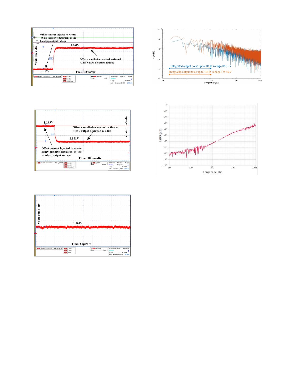
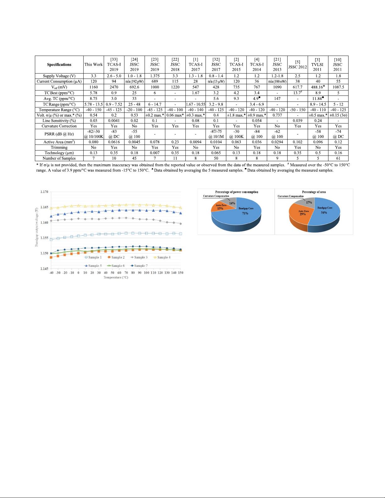
Figs. 8 and 9 show the bandgap output voltage measure-
ment examples during tests with intentionally created offsets.
Initially, the amplifier imbalances generate bandgap voltage
errors of −46 mV and +31 mV. These shifts are reduced to
below 1 mV after activation of the shared auto-zeroing cir-
cuit. Fig. 10 displays the steady-state bandgap output voltage
measured with automatic offset compensation. The b andgap
output spectra without and with offset cancellation are shown
in Fig. 11. Based on noise simulations, both amplifiers under
calibration together have the most dominant noise contribution
Authorized licensed use limited to: Zhejiang University. Downloaded on April 07,2021 at 09:59:51 UTC from IEEE Xplore. Restrictions apply.
