没有合适的资源?快使用搜索试试~ 我知道了~
首页I2C-bus specification-version-2.0.pdf英文版
资源详情
资源评论
资源推荐

THE I
2
C-BUS SPECIFICATION
VERSION 2.0
DECEMBER 1998

2
Philips Semiconductors
The I
2
C-bus specification
CONTENTS
1 PREFACE 3
1.1 Version 1.0- 1992 3
1.2 Version 2.0- 1998 3
1.3 Purchase of Philips I
2
C-bus components 3
2 THE I
2
C-BUS BENEFITS DESIGNERS
AND MANUFACTURERS 4
2.1 Designer benefits 4
2.2 Manufacturer benefits 6
3 INTRODUCTION TO THE I
2
C-BUS
SPECIFICATION 6
4 THE I
2
C-BUS CONCEPT 6
5 GENERAL CHARACTERISTICS 8
6 BIT TRANSFER 8
6.1 Data validity 8
6.2 START and STOP conditions 9
7 TRANSFERRING DATA 10
7.1 Byte format 10
7.2 Acknowledge 10
8 ARBITRATION AND CLOCK
GENERATION 11
8.1 Synchronization 11
8.2 Arbitration 12
8.3 Use of the clock synchronizing
mechanism as a handshake 13
9 FORMATS WITH 7-BIT ADDRESSES 13
10 7-BIT ADDRESSING 15
10.1 Definition of bits in the first byte 15
10.1.1 General call address 16
10.1.2 START byte 17
10.1.3 CBUS compatibility 18
11 EXTENSIONS TO THE STANDARD-
MODE I
2
C-BUS SPECIFICATION 19
12 FAST-MODE 19
13 Hs-MODE 20
13.1 High speed transfer 20
13.2 Serial data transfer format in Hs-mode 21
13.3 Switching from F/S- to Hs-mode and back 23
13.4Hs-mode devices at lower speed modes24
13.5 Mixed speed modes on one serial
bus system 24
13.5.1 F/S-mode transfer in a
mixed-speed bus system 25
13.5.2 Hs-mode transfer in a
mixed-speed bus system 25
13.5.3 Timing requirements for the bridge in a
mixed-speed bus system 27
14 10-BIT ADDRESSING 27
14.1 Definition of bits in the first two bytes 27
14.2 Formats with 10-bit addresses 27
14.3 General call address and start byte
with 10-bit addressing 30
15 ELECTRICAL SPECIFICATIONS
AND TIMING FOR I/O STAGES
AND BUS LINES 30
15.1 Standard- and Fast-mode devices 30
15.2 Hs-mode devices 34
16 ELECTRICAL CONNECTIONS OF
I
2
C-BUS DEVICES TO THE BUS LINES 37
16.1 Maximum and minimum values of
resistors R
p
and R
s
for Standard-mode
I
2
C-bus devices 39
17 APPLICATION INFORMATION 41
17.1 Slope-controlled output stages of
Fast-mode I
2
C-bus devices 41
17.2 Switched pull-up circuit for Fast-
mode I
2
C-bus devices 41
17.3 Wiring pattern of the bus lines 42
17.4 Maximum and minimum values of
resistors R
p
and R
s
for Fast-mode
I
2
C-bus devices 42
17.5 Maximum and minimum values of
resistors R
p
and R
s
for Hs-mode
I
2
C-bus devices 42
18 BI-DIRECTIONAL LEVEL SHIFTER
FOR F/S-MODE I
2
C-BUS SYSTEMS 42
18.1 Connecting devices with different
logic levels 43
18.1.1 Operation of level shifter 44
19 DEVELOPMENT TOOLS AVAILABLE
FROM PHILIPS 45
20 SUPPORT LITERATURE 46

3
Philips Semiconductors
The I
2
C-bus specification
1 PREFACE
1.1 Version 1.0 - 1992
This version of the 1992 I
2
C-bus specification includes the
following modifications:
• Programming of a slave address by software has been
omitted. The realization of this feature is rather
complicated and has not been used.
• The “low-speed mode” has been omitted. This mode is,
in fact, a subset of the total I
2
C-bus specification and
need not be specified explicitly.
• The Fast-mode is added. This allows a fourfold increase
of the bit rate up to 400 kbit/s. Fast-mode devices are
downwards compatible i.e. they can be used in a 0 to
100 kbit/s I
2
C-bus system.
• 10-bit addressing is added. This allows 1024 additional
slave addresses.
• Slope control and input filtering for Fast-mode devices is
specified to improve the EMC behaviour.
NOTE: Neither the 100 kbit/s I
2
C-bus system nor the
100 kbit/s devices have been changed.
1.2 Version 2.0 - 1998
The I
2
C-bus has become a de facto world standard that is
now implemented in over 1000 different ICs and licensed
to more than 50 companies. Many of today’s applications,
however, require higher bus speeds and lower supply
voltages. This updated version of the I
2
C-bus specification
meets those requirements and includes the following
modifications:
• The High-speed mode (Hs-mode) is added. This allows
an increase in the bit rate up to 3.4 Mbit/s. Hs-mode
devices can be mixed with Fast- and Standard-mode
devices on the one I
2
C-bus system with bit rates from 0
to 3.4 Mbit/s.
• The low output level and hysteresis of devices with a
supply voltage of 2 V and below has been adapted to
meet the required noise margins and to remain
compatible with higher supply voltage devices.
• The 0.6 V at 6 mA requirement for the output stages of
Fast-mode devices has been omitted.
• The fixed input levels for new devices are replaced by
bus voltage-related levels.
• Application information for bi-directional level shifter is
added.
1.3 Purchase of Philips I
2
C-bus components
Purchase of Philips I
2
C components conveys a license under the Philips’ I
2
C patent to use the
components in the I
2
C system provided the system conforms to the I
2
C specification defined by
Philips.

4
Philips Semiconductors
The I
2
C-bus specification
2 THE I
2
C-BUS BENEFITS DESIGNERS AND
MANUFACTURERS
In consumer electronics, telecommunications and
industrial electronics, there are often many similarities
between seemingly unrelated designs. For example,
nearly every system includes:
• Some intelligent control, usually a single-chip
microcontroller
• General-purpose circuits like LCD drivers, remote I/O
ports, RAM, EEPROM, or data converters
• Application-oriented circuits such as digital tuning and
signal processing circuits for radio and video systems,
or DTMF generators for telephones with tone dialling.
To exploit these similarities to the benefit of both systems
designers and equipment manufacturers, as well as to
maximize hardware efficiency and circuit simplicity, Philips
developed a simple bi-directional 2-wire bus for efficient
inter-IC control. This bus is called the Inter IC or I
2
C-bus.
At present, Philips’ IC range includes more than 150
CMOS and bipolar I
2
C-bus compatible types for
performing functions in all three of the previously
mentioned categories. All I
2
C-bus compatible devices
incorporate an on-chip interface which allows them to
communicate directly with each other via the I
2
C-bus. This
design concept solves the many interfacing problems
encountered when designing digital control circuits.
Here are some of the features of the I
2
C-bus:
• Only two bus lines are required; a serial data line (SDA)
and a serial clock line (SCL)
• Each device connected to the bus is software
addressable by a unique address and simple
master/slave relationships exist at all times; masters can
operate as master-transmitters or as master-receivers
• It’s a true multi-master bus including collision detection
and arbitration to prevent data corruption if two or more
masters simultaneously initiate data transfer
• Serial, 8-bit oriented, bi-directional data transfers can be
made at up to 100 kbit/s in the Standard-mode, up to
400 kbit/s in the Fast-mode, or up to 3.4 Mbit/s in the
High-speed mode
• On-chip filtering rejects spikes on the bus data line to
preserve data integrity
• The number of ICs that can be connected to the same
bus is limited only by a maximum bus capacitance of
400 pF.
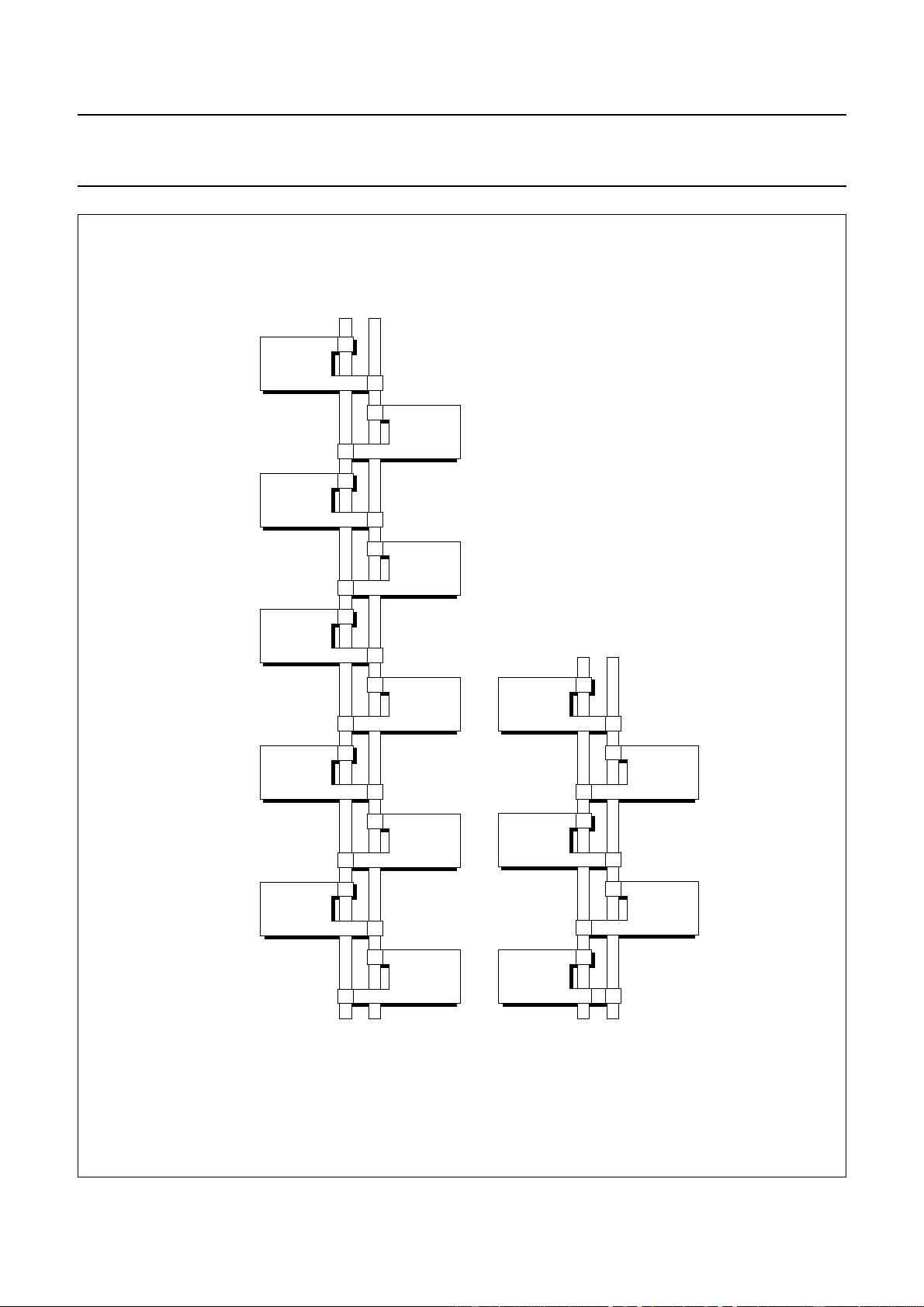
Figure 1 shows two examples of I
2
C-bus applications.
2.1 Designer benefits
I
2
C-bus compatible ICs allow a system design to rapidly
progress directly from a functional block diagram to a
prototype. Moreover, since they ‘clip’ directly onto the
I
2
C-bus without any additional external interfacing, they
allow a prototype system to be modified or upgraded
simply by ‘clipping’ or ‘unclipping’ ICs to or from the bus.
Here are some of the features of I
2
C-bus compatible ICs
which are particularly attractive to designers:
• Functional blocks on the block diagram correspond with
the actual ICs; designs proceed rapidly from block
diagram to final schematic.
• No need to design bus interfaces because the I
2
C-bus
interface is already integrated on-chip.
• Integrated addressing and data-transfer protocol allow
systems to be completely software-defined
• The same IC types can often be used in many different
applications
• Design-time reduces as designers quickly become
familiar with the frequently used functional blocks
represented by I
2
C-bus compatible ICs
• ICs can be added to or removed from a system without
affecting any other circuits on the bus
• Fault diagnosis and debugging are simple; malfunctions
can be immediately traced
• Software development time can be reduced by
assembling a library of reusable software modules.
In addition to these advantages, the CMOS ICs in the
I
2
C-bus compatible range offer designers special features
which are particularly attractive for portable equipment and
battery-backed systems.
They all have:
• Extremely low current consumption
• High noise immunity
• Wide supply voltage range
• Wide operating temperature range.

5
Philips Semiconductors
The I
2
C-bus specification
Fig.1 Two examples of I
2
C-bus applications: (a) a high performance highly-integrated TV set
(b) DECT cordless phone base-station.
handbook, full pagewidth
SDA SCL
MICRO-
CONTROLLER
PCB83C528
PLL
SYNTHESIZER
TSA5512
NON-VOLATILE
MEMORY
PCF8582E
STEREO / DUAL
SOUND
DECODER
TDA9840
HI-FI
AUDIO
PROCESSOR
TDA9860
SINGLE-CHIP
TEXT
SAA52XX
M/S COLOUR
DECODER
TDA9160A
PICTURE
SIGNAL
IMPROVEMENT
TDA4670
VIDEO
PROCESSOR
TDA4685
ON-SCREEN
DISPLAY
PCA8510
(a)
MSB575
SDA SCL
LINE
INTERFACE
PCA1070
BURST MODE
CONTROLLER
PCD5042
ADPCM
PCD5032
(b)
DTMF
GENERATOR
PCD3311
MICRO-
CONTROLLER
P80CLXXX
剩余45页未读,继续阅读


bgnac80211
- 粉丝: 2
- 资源: 26
上传资源 快速赚钱
我的内容管理 收起
我的资源 快来上传第一个资源
我的收益
登录查看自己的收益我的积分 登录查看自己的积分
我的C币 登录后查看C币余额
我的收藏
我的下载
下载帮助

会员权益专享
最新资源
- Xilinx SRIO详解.pptx
- Informatica PowerCenter 10.2 for Centos7.6安装配置说明.pdf
- 现代无线系统射频电路实用设计卷II 英文版.pdf
- 电子产品可靠性设计 自己讲课用的PPT,包括设计方案的可靠性选择,元器件的选择与使用,降额设计,热设计,余度设计,参数优化设计 和 失效分析等
- MPC5744P-DEV-KIT-REVE-QSG.pdf
- 通信原理课程设计报告(ASK FSK PSK Matlab仿真--数字调制技术的仿真实现及性能研究)
- ORIGIN7.0使用说明
- 在VMware Player 3.1.3下安装Redhat Linux详尽步骤
- python学生信息管理系统实现代码
- 西门子MES手册 13 OpcenterEXCR_PortalStudio1_81RB1.pdf
资源上传下载、课程学习等过程中有任何疑问或建议,欢迎提出宝贵意见哦~我们会及时处理!
点击此处反馈


安全验证
文档复制为VIP权益,开通VIP直接复制

评论0