
PFC Handbook
http://onsemi.com
92
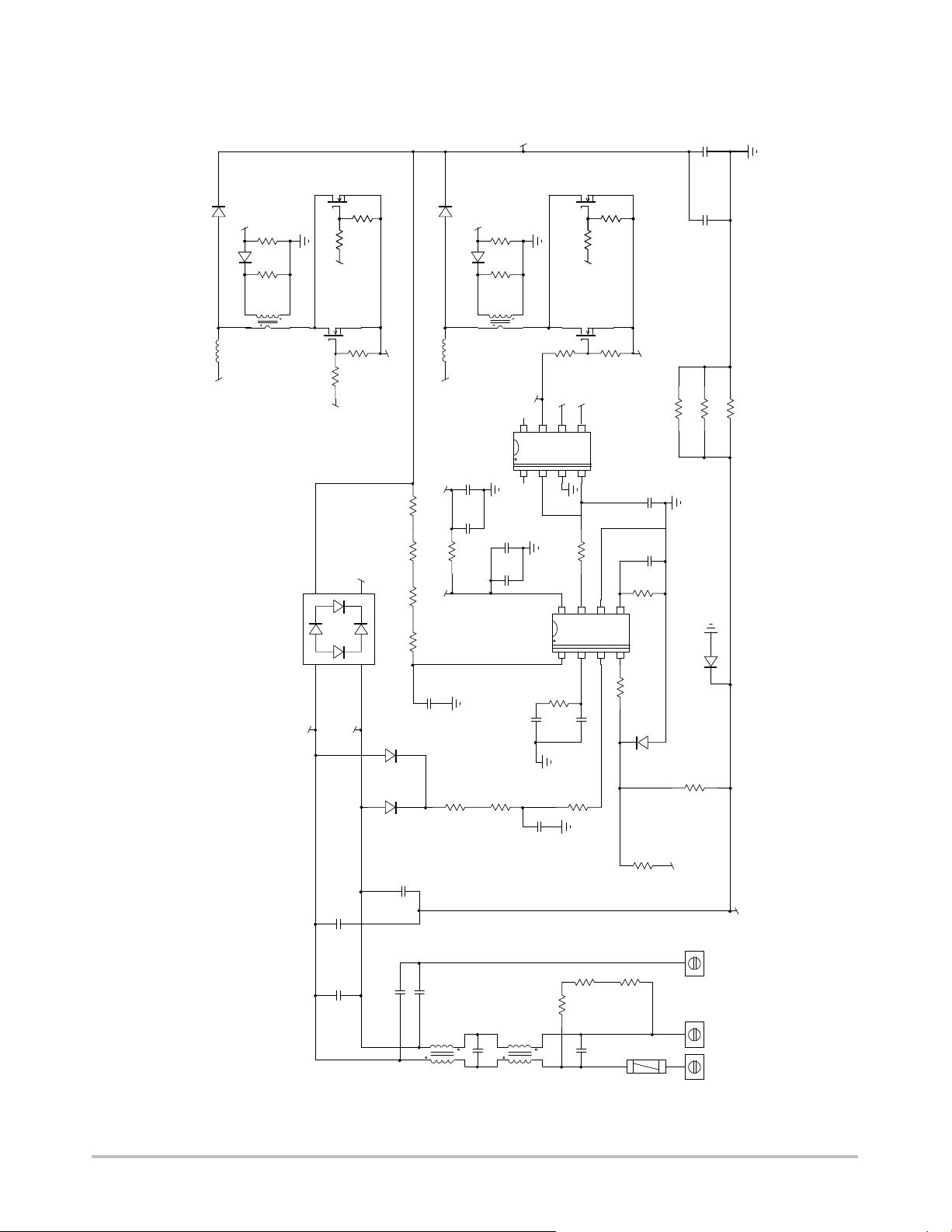
Circuit Schematics
L4
0. 2m
R2
2700k
PH 2
L1
0. 2m
PH 1
D2x
1N 4007
1
2
3
4
8
6
7
N C P1653
FB
Vctrl
In
CS
VCC
Drv
GND
Vm
X5
NCP1653
D1
1N 4007
R7
56k
C4
1nF
R3
470k
C1
100 nF /
63 V
C2
100nF
R8
100m / 3W
R4
2. 2k
R1
2200k
X1
SPP20N60
R17
10
PH 2
R15
10
R20x
10k
D3
1N 5817
R5
390
X2
SPP20N60
R18
10
R19
10k
R9
100m / 3W
R10
100m / 3W
RETURN
R13x
680k
R14
390k
R12
680k
R11
180k
C5
10nF
90 to 265 Vrms
5 0 or 60 Hz line volt a ge
C13
1 mF
Type = X2
CM 2
F1
10 A
LN Earth
C19
4. 7 nF
Type = Y2
C18
4. 7 nF
Type = Y2
C15
1mF
Type = X2
CM 1
C16
1mF
C17
1mF
R21x
680k
+
−
IN
X4
D iode bridge
RETURN
PH 1
28
C3
220nF
R6
100k
C6
22mF
R22x
680k
R23x
680k
C14
1 mF
Type = X2
C24
220nF
C25
22mF
M C 33152
NC
In A
GND
In B
NC
Ou tA
Ou tB
VCC
DRV1
R13
100
C27
100pF
DRV1
VCC 2
C28
220nF
VCC 2
VCC
DRV2
RETURN
RETURN
R24
2. 2k
CS
D5
1N 5406
Figure 7−10. Application Schematic
N
5
1
2
3
4
8
6
7
5
X7
SPP20N60
X3
SPP20N60
R23
10k
R22
10
R28
3
R25
15k
CS
D7
CSD10060
R28
3
R29
15k
CS
1N4148
D2
1N4148
D4
D8
CSD10060
V
out
R21
10k
R20
10
++
C11
330 m/450 V
C12
330 m/450 V
DRV2
DRV1


剩余37页未读,继续阅读

weixin_38744435
- 粉丝: 370
- 资源: 2万+
 我的内容管理
收起
我的内容管理
收起
- 我的资源
快来上传第一个资源
 我的收益 登录查看自己的收益
 我的积分
登录查看自己的积分
我的积分
登录查看自己的积分
 我的C币
登录后查看C币余额
我的C币
登录后查看C币余额
 我的收藏
我的收藏  我的下载
我的下载  下载帮助
下载帮助

会员权益专享


最新资源
- RTL8188FU-Linux-v5.7.4.2-36687.20200602.tar(20765).gz
- c++校园超市商品信息管理系统课程设计说明书(含源代码) (2).pdf
- 建筑供配电系统相关课件.pptx
- 企业管理规章制度及管理模式.doc
- vb打开摄像头.doc
- 云计算-可信计算中认证协议改进方案.pdf
- [详细完整版]单片机编程4.ppt
- c语言常用算法.pdf
- c++经典程序代码大全.pdf
- 单片机数字时钟资料.doc
- 11项目管理前沿1.0.pptx
- 基于ssm的“魅力”繁峙宣传网站的设计与实现论文.doc
- 智慧交通综合解决方案.pptx
- 建筑防潮设计-PowerPointPresentati.pptx
- SPC统计过程控制程序.pptx
- SPC统计方法基础知识.pptx
资源上传下载、课程学习等过程中有任何疑问或建议,欢迎提出宝贵意见哦~我们会及时处理!
点击此处反馈


评论0