没有合适的资源?快使用搜索试试~ 我知道了~
首页MT29F4G08ABAWP
MT29F4G08ABAWP
需积分: 9 148 浏览量
更新于2023-05-22
评论
收藏 1.31MB PDF 举报
Micron NAND Flash devices include an asynchronous data interface for high-performance I/O operations. These devices use a highly multiplexed 8-bit bus (I/Ox) to transfer commands, address, and data. There are five control signals used to implement the asynchronous data interface: CE#, CLE, ALE, WE#,
资源详情
资源评论
资源推荐

NAND Flash Memory
MT29F4G08ABADAH4, MT29F4G08ABADAWP, MT29F4G08ABBDAH4,
MT29F4G08ABBDAHC, MT29F4G16ABADAH4, MT29F4G16ABADAWP,
MT29F4G16ABBDAH4, MT29F4G16ABBDAHC, MT29F8G08ADADAH4,
MT29F8G08ADBDAH4, MT29F8G16ADADAH4, MT29F8G16ADBDAH4,
MT29F16G08AJADAWP
Features
• Open NAND Flash Interface (ONFI) 1.0-compliant
1
• Single-level cell (SLC) technology
• Organization
– Page size x8: 2112 bytes (2048 + 64 bytes)
– Page size x16: 1056 words (1024 + 32 words)
– Block size: 64 pages (128K + 4K bytes)
– Plane size: 2 planes x 2048 blocks per plane
– Device size: 4Gb: 4096 blocks; 8Gb: 8192 blocks
16Gb: 16,384 blocks
• Asynchronous I/O performance
–
t
RC/
t
WC: 20ns (3.3V), 25ns (1.8V)
• Array performance
– Read page: 25µs
3
– Program page: 200µs (TYP: 1.8V, 3.3V)
3
– Erase block: 700µs (TYP)
• Command set: ONFI NAND Flash Protocol
• Advanced command set
– Program page cache mode
4
– Read page cache mode
4
– One-time programmable (OTP) mode
– Two-plane commands
4
– Interleaved die (LUN) operations
– Read unique ID
– Block lock (1.8V only)
– Internal data move
• Operation status byte provides software method for
detecting
– Operation completion
– Pass/fail condition
– Write-protect status
• Ready/Busy# (R/B#) signal provides a hardware
method of detecting operation completion
• WP# signal: Write protect entire device
• First block (block address 00h) is valid when ship-
ped from factory with ECC. For minimum required
ECC, see Error Management.
• Block 0 requires 1-bit ECC if PROGRAM/ERASE cy-
cles are less than 1000
• RESET (FFh) required as first command after pow-
er-on
• Alternate method of device initialization (Nand_In-
it) after power up (contact factory)
• Internal data move operations supported within the
plane from which data is read
• Quality and reliability
– Data retention: 10 years
– Endurance: 100,000 PROGRAM/ERASE cycles
• Operating voltage range
– V
CC
: 2.7–3.6V
– V
CC
: 1.7–1.95V
• Operating temperature:
– Commercial: 0°C to +70°C
– Industrial (IT): –40ºC to +85ºC
• Package
– 48-pin TSOP type 1, CPL
2
– 63-ball VFBGA
Notes:
1. The ONFI 1.0 specification is available at
www.onfi.org.
2. CPL = Center parting line.
3. See Program and Erase Characteristics for
t
R_ECC and
t
PROG_ECC specifications.
4. These commands supported only with ECC
disabled.
Micron Confidential and Proprietary
4Gb, 8Gb, 16Gb: x8, x16 NAND Flash Memory
Features
PDF: 09005aef83b25735
m60a_4gb_8gb_16gb_ecc_nand.pdf - Rev. N 10/12 EN
1
Micron Technology, Inc. reserves the right to change products or specifications without notice.
© 2009 Micron Technology, Inc. All rights reserved.
Products and specifications discussed herein are subject to change by Micron without notice.
捷多邦,您值得信赖的PCB打样专家!

Part Numbering Information
Micron NAND Flash devices are available in different configurations and densities. Verify valid part numbers by
using Micron’s part catalog search at www.micron.com. To compare features and specifications by device type,
visit www.micron.com/products. Contact the factory for devices not found.
Figure 1: Marketing Part Number Chart
MT 29F 4G 08 A B A D A WP IT ES :D
Micron Technology
Product Family
29F = NAND Flash memory
Density
4G = 4Gb
8G = 8Gb
16G = 16Gb
Device Width
08 = 8-bit
16 = 16-bit
Level
A = SLC
Classification
Mark Die nCE RnB I/O Channels
B 1 1 1 1
D 2 1 1 1
Operating Voltage Range
A = 3.3V (2.7–3.6V)
B = 1.8V (1.7–1.95V)
Feature Set
D = Feature set D
Design Revision (shrink)
Production Status
Blank = Production
ES = Engineering sample
MS = Mechanical sample
QS = Qualification sample
Special Options
Blank
X = Product longevity program (PLP)
Operating Temperature Range
Blank = Commercial (0°C to +70°C)
IT = Industrial (–40°C to +85°C)
Speed Grade
Blank
Package Code
WP = 48-pin TSOP 1
HC = 63-ball VFBGA (10.5 x 13 x 1.0mm)
H4 = 63-ball VFBGA (9 x 11 x 1.0mm)
Interface
A = Async only
J 4 2 12
Micron Confidential and Proprietary
4Gb, 8Gb, 16Gb: x8, x16 NAND Flash Memory
Features
PDF: 09005aef83b25735
m60a_4gb_8gb_16gb_ecc_nand.pdf - Rev. N 10/12 EN
2
Micron Technology, Inc. reserves the right to change products or specifications without notice.
© 2009 Micron Technology, Inc. All rights reserved.

Contents
General Description ......................................................................................................................................... 8
Signal Descriptions ........................................................................................................................................... 8
Signal Assignments ........................................................................................................................................... 9
Package Dimensions ....................................................................................................................................... 12
Architecture ................................................................................................................................................... 15
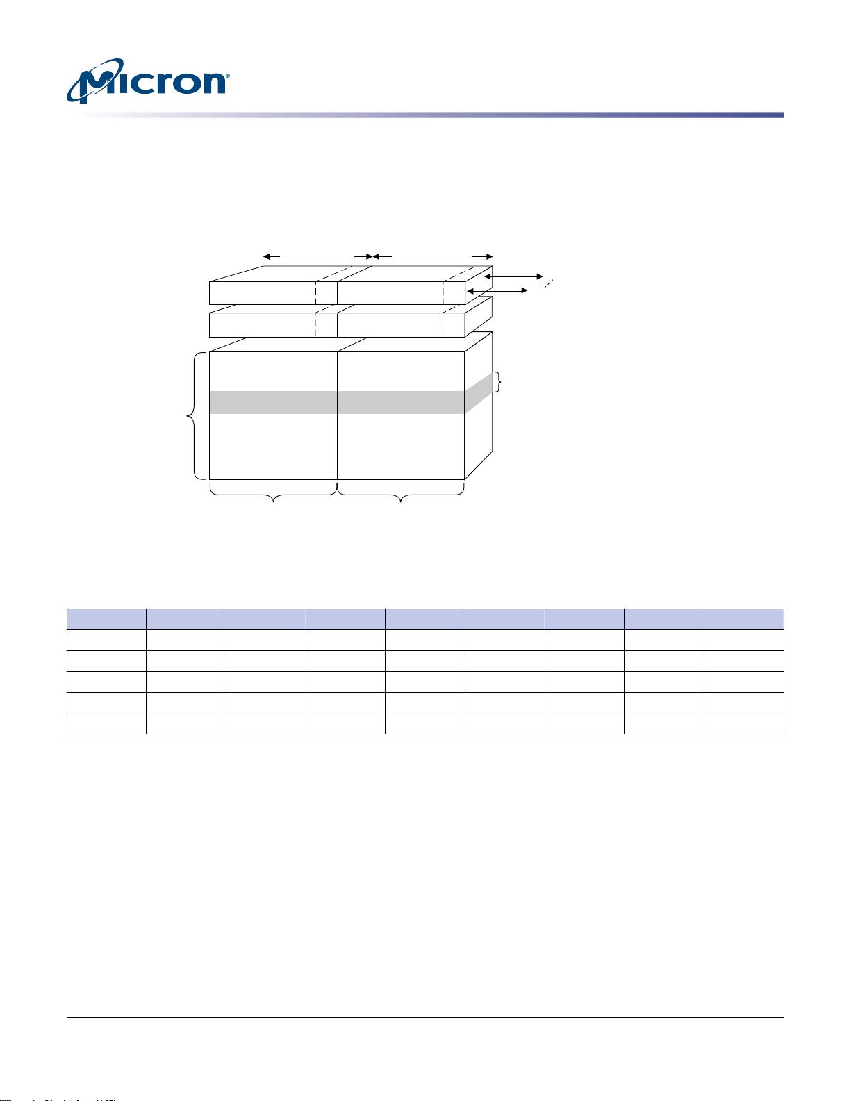
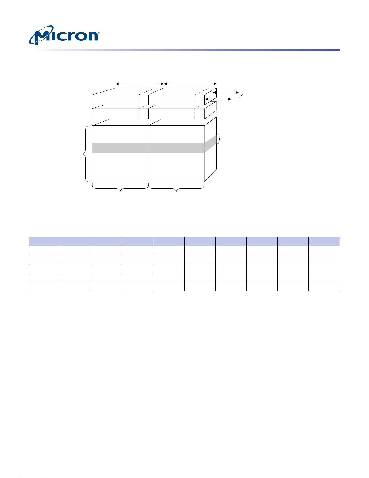
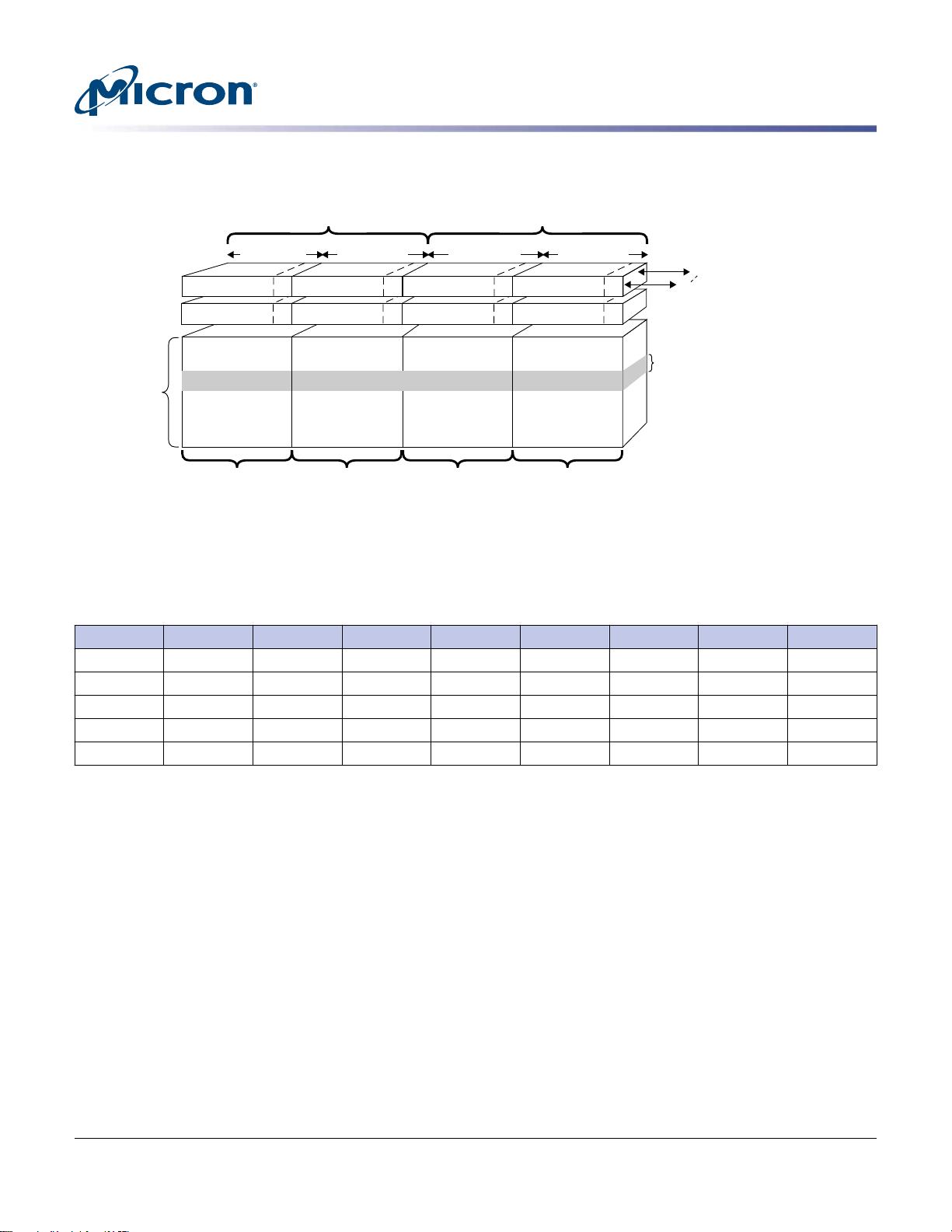
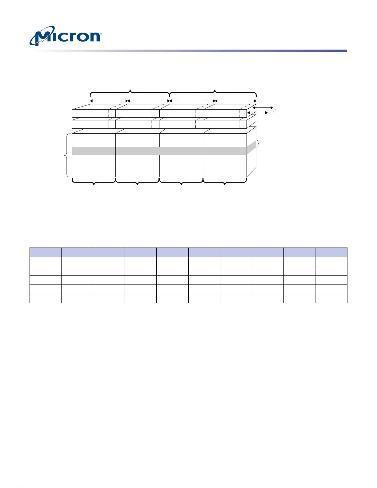
Device and Array Organization
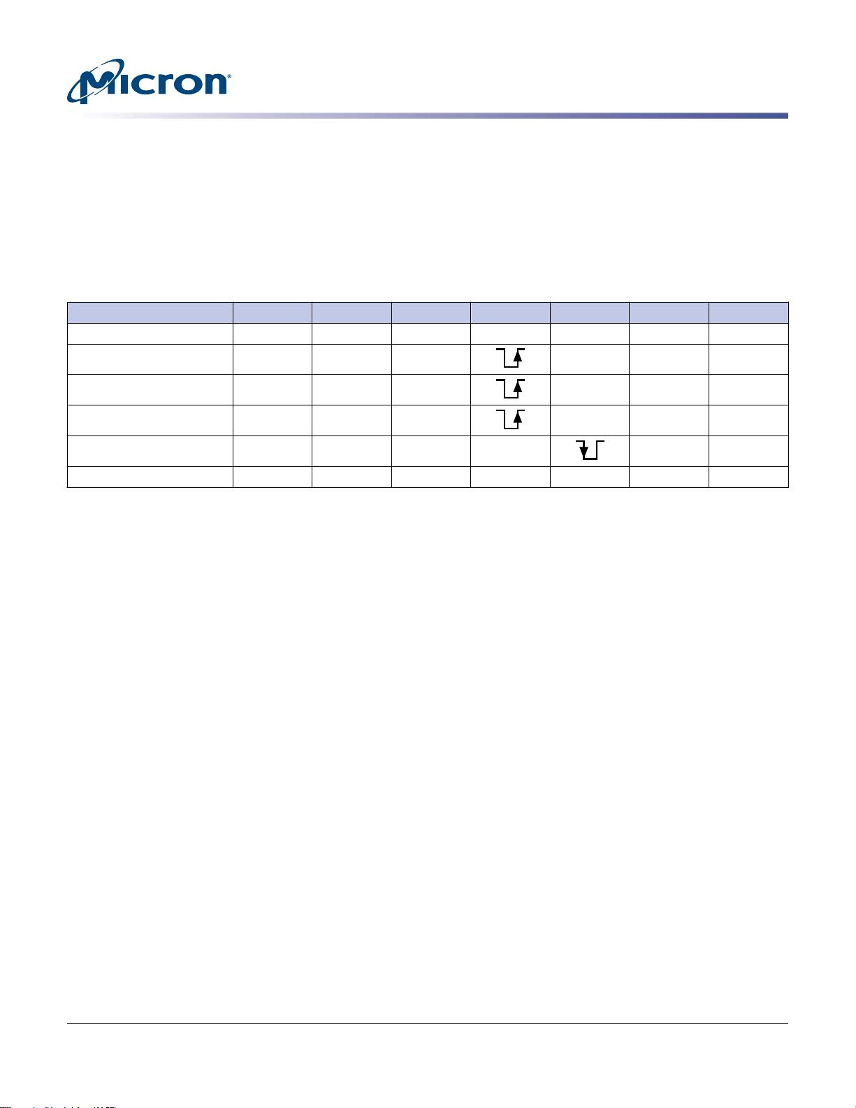
 ........................................................................................................................ 16
Asynchronous Interface Bus Operation ........................................................................................................... 20
Asynchronous Enable/Standby ................................................................................................................... 20
Asynchronous Commands .......................................................................................................................... 20
Asynchronous Addresses ............................................................................................................................ 22
Asynchronous Data Input ........................................................................................................................... 23
Asynchronous Data Output ......................................................................................................................... 24
Write Protect# ............................................................................................................................................ 25
Ready/Busy# .............................................................................................................................................. 25
Device Initialization ....................................................................................................................................... 30
Command Definitions .................................................................................................................................... 31
Reset Operations ............................................................................................................................................ 34
RESET (FFh) ............................................................................................................................................... 34
Identification Operations ................................................................................................................................ 35
READ ID (90h) ............................................................................................................................................ 35
READ ID Parameter Tables .............................................................................................................................. 36
READ PARAMETER PAGE (ECh) ...................................................................................................................... 39
Parameter Page Data Structure Tables ............................................................................................................. 40
Bare Die Parameter Page Data Structure Tables ................................................................................................ 45
READ UNIQUE ID (EDh) ................................................................................................................................ 48
Feature Operations ......................................................................................................................................... 49
SET FEATURES (EFh) .................................................................................................................................. 50
GET FEATURES (EEh) ................................................................................................................................. 51
Status Operations ........................................................................................................................................... 54
READ STATUS (70h) ................................................................................................................................... 55
READ STATUS ENHANCED (78h) ................................................................................................................ 55
Column Address Operations ........................................................................................................................... 57
RANDOM DATA READ (05h-E0h) ................................................................................................................ 57
RANDOM DATA READ TWO-PLANE (06h-E0h) ............................................................................................ 58
RANDOM DATA INPUT (85h) ...................................................................................................................... 59
PROGRAM FOR INTERNAL DATA INPUT (85h) ........................................................................................... 60
Read Operations ............................................................................................................................................. 62
READ MODE (00h) ..................................................................................................................................... 64
READ PAGE (00h-30h) ................................................................................................................................ 64
READ PAGE CACHE SEQUENTIAL (31h) ...................................................................................................... 65
READ PAGE CACHE RANDOM (00h-31h) .................................................................................................... 66
READ PAGE CACHE LAST (3Fh) .................................................................................................................. 68
READ PAGE TWO-PLANE 00h-00h-30h ....................................................................................................... 69
Program Operations ....................................................................................................................................... 71
PROGRAM PAGE (80h-10h) ......................................................................................................................... 72
PROGRAM PAGE CACHE (80h-15h) ............................................................................................................. 72
PROGRAM PAGE TWO-PLANE (80h-11h) .................................................................................................... 75
Erase Operations ............................................................................................................................................ 77
ERASE BLOCK (60h-D0h) ............................................................................................................................ 77
ERASE BLOCK TWO-PLANE (60h-D1h) ....................................................................................................... 78
Micron Confidential and Proprietary
4Gb, 8Gb, 16Gb: x8, x16 NAND Flash Memory
Features
PDF: 09005aef83b25735
m60a_4gb_8gb_16gb_ecc_nand.pdf - Rev. N 10/12 EN
3
Micron Technology, Inc. reserves the right to change products or specifications without notice.
© 2009 Micron Technology, Inc. All rights reserved.

Internal Data Move Operations ....................................................................................................................... 79
READ FOR INTERNAL DATA MOVE (00h-35h) ............................................................................................. 80
PROGRAM FOR INTERNAL DATA MOVE (85h–10h) ..................................................................................... 81
PROGRAM FOR INTERNAL DATA MOVE TWO-PLANE (85h-11h) ................................................................. 82
Block Lock Feature ......................................................................................................................................... 83
WP# and Block Lock ................................................................................................................................... 83
UNLOCK (23h-24h) .................................................................................................................................... 83
LOCK (2Ah) ................................................................................................................................................ 86
LOCK TIGHT (2Ch) ..................................................................................................................................... 87
BLOCK LOCK READ STATUS (7Ah) .............................................................................................................. 88
One-Time Programmable (OTP) Operations .................................................................................................... 90
Legacy OTP Commands .............................................................................................................................. 90
OTP DATA PROGRAM (80h-10h) ................................................................................................................. 91
RANDOM DATA INPUT (85h) ...................................................................................................................... 92
OTP DATA PROTECT (80h-10) ..................................................................................................................... 93
OTP DATA READ (00h-30h) ......................................................................................................................... 95
Two-Plane Operations .................................................................................................................................... 97
Two-Plane Addressing ................................................................................................................................ 97
Interleaved Die (Multi-LUN) Operations ......................................................................................................... 106
Error Management ........................................................................................................................................ 107
Internal ECC and Spare Area Mapping for ECC ............................................................................................... 109
Electrical Specifications ................................................................................................................................. 111
Electrical Specifications – DC Characteristics and Operating Conditions .......................................................... 113
Electrical Specifications – AC Characteristics and Operating Conditions .......................................................... 115
Electrical Specifications – Program/Erase Characteristics ................................................................................ 118
Asynchronous Interface Timing Diagrams ...................................................................................................... 119
Revision History ............................................................................................................................................ 131
Rev. N – 10/12 ............................................................................................................................................ 131
Rev. M – 02/12 ........................................................................................................................................... 131
Rev. L – 1/12 .............................................................................................................................................. 131
Rev. K – 11/11 ............................................................................................................................................ 131
Rev. J – 09/11 ............................................................................................................................................. 131
Rev. I – 07/11 ............................................................................................................................................. 131
Rev. H – 12/10 ............................................................................................................................................ 131
Rev. G – 10/10 ............................................................................................................................................ 131
Rev. F – 06/10 ............................................................................................................................................ 131
Rev. E – 05/10 ............................................................................................................................................ 131
Rev. D – 03/10 ............................................................................................................................................ 132
Rev. C – 01/10 ............................................................................................................................................ 132
Rev. B – 10/09 ............................................................................................................................................ 132
Rev. A – 07/09 ............................................................................................................................................ 132
Micron Confidential and Proprietary
4Gb, 8Gb, 16Gb: x8, x16 NAND Flash Memory
Features
PDF: 09005aef83b25735
m60a_4gb_8gb_16gb_ecc_nand.pdf - Rev. N 10/12 EN
4
Micron Technology, Inc. reserves the right to change products or specifications without notice.
© 2009 Micron Technology, Inc. All rights reserved.

List of Tables
Table 1: Signal Definitions ............................................................................................................................... 8
Table 2: Array Addressing – MT29F4G08 (x8) .................................................................................................. 16
Table 3: Array Addressing – MT29F4G16 (x16) ................................................................................................. 17
Table 4: Array Addressing – MT29F8G08 and MT29F16G08 (x8) ....................................................................... 18
Table 5: Array Addressing – MT29F8G16 ( x16) ................................................................................................ 19
Table 6: Asynchronous Interface Mode Selection ............................................................................................ 20
Table 7: Command Set .................................................................................................................................. 31
Table 8: Two-Plane Command Set .................................................................................................................. 33
Table 9: READ ID Parameters for Address 00h ................................................................................................. 36
Table 10: READ ID Parameters for Address 20h ............................................................................................... 38
Table 11: Parameter Page Data Structure ........................................................................................................ 40
Table 12: Parameter Page Data Structure ........................................................................................................ 45
Table 13: Feature Address Definitions ............................................................................................................. 49
Table 14: Feature Address 90h – Array Operation Mode ................................................................................... 50
Table 15: Feature Addresses 01h: Timing Mode ............................................................................................... 52
Table 16: Feature Addresses 80h: Programmable I/O Drive Strength ................................................................ 53
Table 17: Feature Addresses 81h: Programmable R/B# Pull-Down Strength ...................................................... 53
Table 18: Status Register Definition ................................................................................................................ 54
Table 19: Block Lock Address Cycle Assignments ............................................................................................ 85
Table 20: Block Lock Status Register Bit Definitions ........................................................................................ 88
Table 21: Error Management Details ............................................................................................................. 107
Table 22: Absolute Maximum Ratings ............................................................................................................ 111
Table 23: Recommended Operating Conditions ............................................................................................. 111
Table 24: Valid Blocks ................................................................................................................................... 111
Table 25: Capacitance ................................................................................................................................... 112
Table 26: Test Conditions .............................................................................................................................. 112
Table 27: DC Characteristics and Operating Conditions (3.3V) ....................................................................... 113
Table 28: DC Characteristics and Operating Conditions (1.8V) ....................................................................... 114
Table 29: AC Characteristics: Command, Data, and Address Input (3.3V) ........................................................ 115
Table 30: AC Characteristics: Command, Data, and Address Input (1.8V) ........................................................ 115
Table 31: AC Characteristics: Normal Operation (3.3V) .................................................................................. 116
Table 32: AC Characteristics: Normal Operation (1.8V) .................................................................................. 116
Table 33: Program/Erase Characteristics ....................................................................................................... 118
Micron Confidential and Proprietary
4Gb, 8Gb, 16Gb: x8, x16 NAND Flash Memory
Features
PDF: 09005aef83b25735
m60a_4gb_8gb_16gb_ecc_nand.pdf - Rev. N 10/12 EN
5
Micron Technology, Inc. reserves the right to change products or specifications without notice.
© 2009 Micron Technology, Inc. All rights reserved.
剩余131页未读,继续阅读


安全验证
文档复制为VIP权益,开通VIP直接复制

评论0