没有合适的资源?快使用搜索试试~ 我知道了~
首页NVMe SSD介绍.pdf
资源详情
资源评论
资源推荐

Chapter 2
SSD Architecture and PCI Express Interface
K. Eshghi and R. Micheloni
Abstract Flash-memory-based solid-state disks (SSDs) provide faster random
access and data transfer rates than electromechanical drives and today can often
serve as rotating-disk replacements, but the host interface to SSDs remains a
performance bottleneck. PCI Express (PCIe)-based SSDs together with an emerging
standard called NVMe (Non-Volatile Memory express) promises to solve the
interface bottleneck.
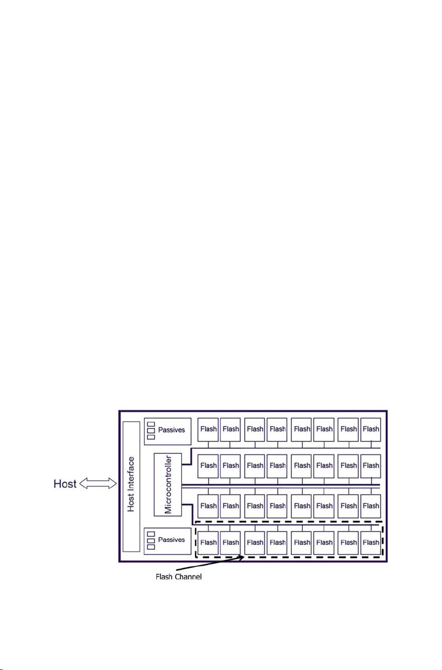
This chapter walks the reader through the SSD block diagram, from the NAND
memory to the Flash controller (including wear leveling, bad block management,
and garbage collection). PCIe basics and different PCIe SSD architectures are
reviewed. Finally, an overview on the standardization effort around PCI Express
is presented.
2.1 Introduction
Creativity is just connecting things. When you ask creative people how they did something,
they feel a little guilty because they didn’t really do it, they just saw something. It seemed
obvious to them after a while.
– Steve Jobs
Solid-state drives promise to greatly enhance enterprise storage performance. While
electromechanical disk drives have continuously ramped in capacity, the rotating-
storage technology doesn’t provide the access-time or transfer-rate performance
required in demanding enterprise applications, including on-line transaction pro-
cessing, data mining, and cloud computing. Client applications are also in need of
K. Eshghi () • R. Micheloni
Enterprise Computing Division, Integrated Device Technology, Inc.,
San Jose, CA, USA
e-mail: kamyar.eshghi@alum.mit.edu; rino.micheloni@ieee.org
R. Micheloni et al., Inside Solid State Drives (SSDs), Springer Series
in Advanced Microelectronics 37, DOI 10.1007/978-94-007-5146-0
2,
© Springer ScienceCBusiness Media Dordrecht 2013
19

20 K. Eshghi and R. Micheloni
an alternative to electromechanical disk drives that can deliver faster response times,
use less power, and fit in smaller mobile form factors.
Flash-memory-based Solid-State Disks (SSDs) can offer much faster random
access to data and faster transfer rates. Moreover, SSD capacity is now at the point
that the drives can serve as rotating-disk replacements. But for many applications
the host interface to SSDs remains a bottleneck to performance. PCI Express
(PCIe)-based SSDs together with emerging host control interface standards address
this interface bottleneck. SSDs with legacy storage interfaces are proving useful,
and PCIe SSDs will further increase performance and improve responsiveness by
connecting directly to the host processor.
2.2 SSD Architecture
Flash cards, USB keys and Solid State Disks are definitely the most known examples
of electronic systems based on non-volatile memories, especially of NAND type
(Sect. 2.4).
Several types of memory cards (CF, SD, MMC, :::) are available in the market
[1–3], with different user interfaces and form factors, depending on the needs of
the target application: e.g. mobile phones need very small-sized removable media
like SD.
SSDs are the emerging application for NAND. A SSD is a complete, small sys-
tem where every component is soldered on a PCB and is independently packaged:
NANDs are usually available in TSOP packages.
A basic block diagram of solid state disk is shown in Fig. 2.1. In addition to
memories and a controller, there are usually other components. For instance, an
Fig. 2.1 Block diagram of a SSD

2 SSD Architecture and PCI Express Interface 21
external DC-DC converter can be added in order to derive the internal power supply,
or a quartz can be used for a better clock precision. Of course, reasonable filter
capacitors are inserted for stabilizing the power supply. It is also very common to
have a temp sensor for power management reasons. For data caching, a fast DDR
memory is frequently used: during a write access, the cache is used for storing data
before transfer to the Flash. The benefit is that data updating, e.g. in routing tables,
is faster and does not wear out the Flash.
In order to improve performances, NANDs are organized in different Flash
channels, as shown in Fig. 2.1.
2.3 Non-volatile Memories
Semiconductor memories can be divided into two major categories: RAM (Random
Access Memories)andROM(Read Only Memories): RAMs lose their content
when power supply is switched off, while ROMs virtually hold it forever. A third
category lies in between, i.e. NVM (Non-Volatile Memories), whose content can be
electrically altered but it is also preserved when the power supply is switched off.
NVMs are more flexible than the original ROM, whose content is defined during
manufacturing and cannot be changed by the user anymore.
NVM’s history began in the 1970s, with the introduction of the first EPROM
memory (Erasable Programmable Read Only Memory). In the early 1990s, Flash
memories came into the game and they started being used in portable products,
like mobile phones, USB keys, camcorders, and digital cameras. Solid State Disk
(SSD) is the latest killer application for Flash memories. It is worth mentioning that,
depending on how the memory cells are organized in the memory array, it is possible
to distinguish between NAND and NOR Flash memories. In this book we focus on
NAND memories as they are one of the basic elements of SSDs. NOR architecture
is described in great details in [4].
NAND Flash cell is based on the Floating Gate (FG) technology, whose cross
section is shown in Fig. 2.2. A MOS transistor is built with two overlapping gates
Control Gate (CG)
Drain (D)
Source (S)
Floating Gate (FG)
Tunnel Oxide (TOX)
Interpoly Oxide
(D) (B) (S)
(FG)
(CG)
Bulk (B)
C
PP
C
S
C
B
C
D
Fig. 2.2 Schematic representation of a floating gate memory cell (left) and the corresponding
capacitive model (right)

22 K. Eshghi and R. Micheloni
rather than a single one: the first one is completely surrounded by oxide, while
the second one is contacted to form the gate terminal. The isolated gate constitutes
an excellent “trap” for electrons, which guarantees charge retention for years. The
operations performed to inject and remove electrons from the isolated gate are called
program and erase, respectively. These operations modify the threshold voltage V
TH
of the memory cell, which is a special type of MOS transistor. Applying a fixed
voltage to cell’s terminals, it is then possible to discriminate two storage levels:
when the gate voltage is higher than the cell’s V
TH
, the cell is on (“1”), otherwise it
is off (“0”).
It is worth mentioning that, due to floating gate scalability reasons, charge trap
memories are gaining more and more attention and they are described in Chap. 5,
together with their 3D evolution.
2.4 NAND Flash
2.4.1 NAND Array
A Flash device contains an array of floating-gate transistors: each of them acts as
memory cell. In Single Level Cell (SLC) devices, each memory cell stores one bit
of information; Multi-Level Cell (MLC) devices store 2 bits per cell.
The basic element of a NAND Flash memory is the NAND string, as shown
in Fig. 2.3a. Usually, a string is made up by 32 (M
C0
to M
C31
), 64 or 128 cells
connected in series. Two selection transistors are placed at the edges of the string:
M
SSL
ensures the connection to the source line. M
DSL
connects the string to the
bitline BL. The cell’s control gates are connected through the wordlines (WLs).
Figure 2.3b shows how the matrix array is built starting from the basic string. In the
WL direction, adjacent NAND strings share the same WL, DSL, BSL and SL. In
the BL direction, two consecutive strings share the bitline contact. Figure 2.4 shows
a section of the NAND array along the bitline direction.
All the NAND strings sharing the same group of WL’s form a Block. In Fig. 2.3b
there are three blocks:
–BLOCK0ismadeupbyWL
0
< 31:0>;
–BLOCK1ismadeupbyWL
1
< 31:0>;
–BLOCK2ismadeupbyWL
2
< 31:0 > .
Logical pages are made up of cells belonging to the same WL. The number of
pages per WL is related to the storage capabilities of the memory cell. Depending
on the number of storage levels, Flash memories are referred to in different ways:
• SLC memories stores 1 bit per cell;
• MLC memories stores 2 bits per cell;
• 8LC memories stores 3 bits per cell;
• 16LC memories stores 4 bits per cell.

2 SSD Architecture and PCI Express Interface 23
M
BSL
M
SSL
WL<0>
BSL
SSL
WL<31>
WL<30>
Bitline (BL)
M
C0
M
C30
M
C31
D
S
Source Line (SL)
D
S
BSL
0
WL
0
<31:0>
SSL
0
SL
BLe
NAND String
D
S
BLo
NAND String
SSL
1
DSL
1
S
D
NAND String
S
D
NAND String
WL
1
<31:0>
BLOCK 0 BLOCK 1
DSL
2
SSL
2
S
NAND String
S
NAND String
WL
2
<31:0>
BLOCK 2
ab
Fig. 2.3 NAND String (a) and NAND array (b)
Fig. 2.4 NAND array section along the bitline direction
剩余27页未读,继续阅读


安全验证
文档复制为VIP权益,开通VIP直接复制

评论0