没有合适的资源?快使用搜索试试~ 我知道了~
首页TJA1043 datasheet REV6
资源详情
资源评论
资源推荐

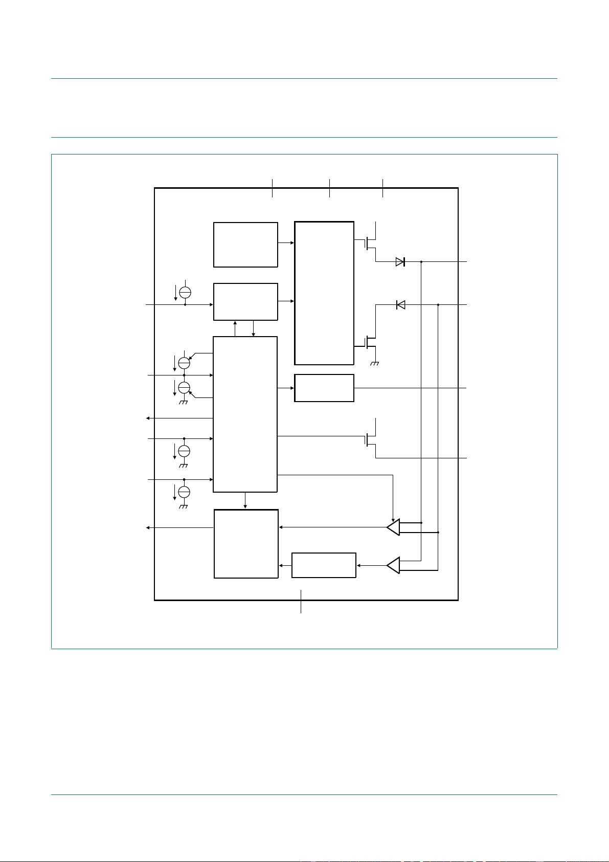
1. General description
The TJA1043 high-speed CAN transceiver provides an interface between a Controller
Area Network (CAN) protocol controller and the physical two-wire CAN bus. The
transceiver is designed for high-speed CAN applications in the automotive industry,
providing differential transmit and receive capability to (a microcontroller with) a CAN
protocol controller.
The TJA1043 belongs to the third generation of high-speed CAN transceivers from NXP
Semiconductors, offering significant improvements over first- and second-generation
devices such as the TJA1041A. It offers improved ElectroMagnetic Compatibility (EMC)
and ElectroStatic Discharge (ESD) performance, very low power consumption, and
passive behavior when the supply voltage is turned off. Advanced features include:
• Low-power management controls the power supply throughout the node while
supporting local and remote wake-up with wake-up source recognition
• Several protection and diagnostic functions including bus line short-circuit detection
and battery connection detection
• Can be interfaced directly to microcontrollers with supply voltages from 3 V to 5 V
The TJA1043 implements the CAN physical layer as defined in ISO 11898-2:2016 and
SAE J2284-1 to SAE J2284-5. This implementation enables reliable communication in the
CAN FD fast phase at data rates up to 5 Mbit/s.
These features make the TJA1043 the ideal choice for high speed CAN networks
containing nodes that need to be available all times, even when the internal V
IO
and V
CC
supplies are switched off.
2. Features and benefits
2.1 General
ISO 11898-2:2016 and SAE J2284-1 to SAE J2284-5 compliant
Loop delay symmetry timing enables reliable communication at data rates up to
5 Mbit/s in the CAN FD fast phase
Suitable for 12 V and 24 V systems
Low ElectroMagnetic Emission (EME) and high ElectroMagnetic Immunity (EMI)
V
IO
input allows for direct interfacing with 3 V and 5 V microcontrollers
SPLIT voltage output for stabilizing the recessive bus level
Listen-only mode for node diagnosis and failure containment
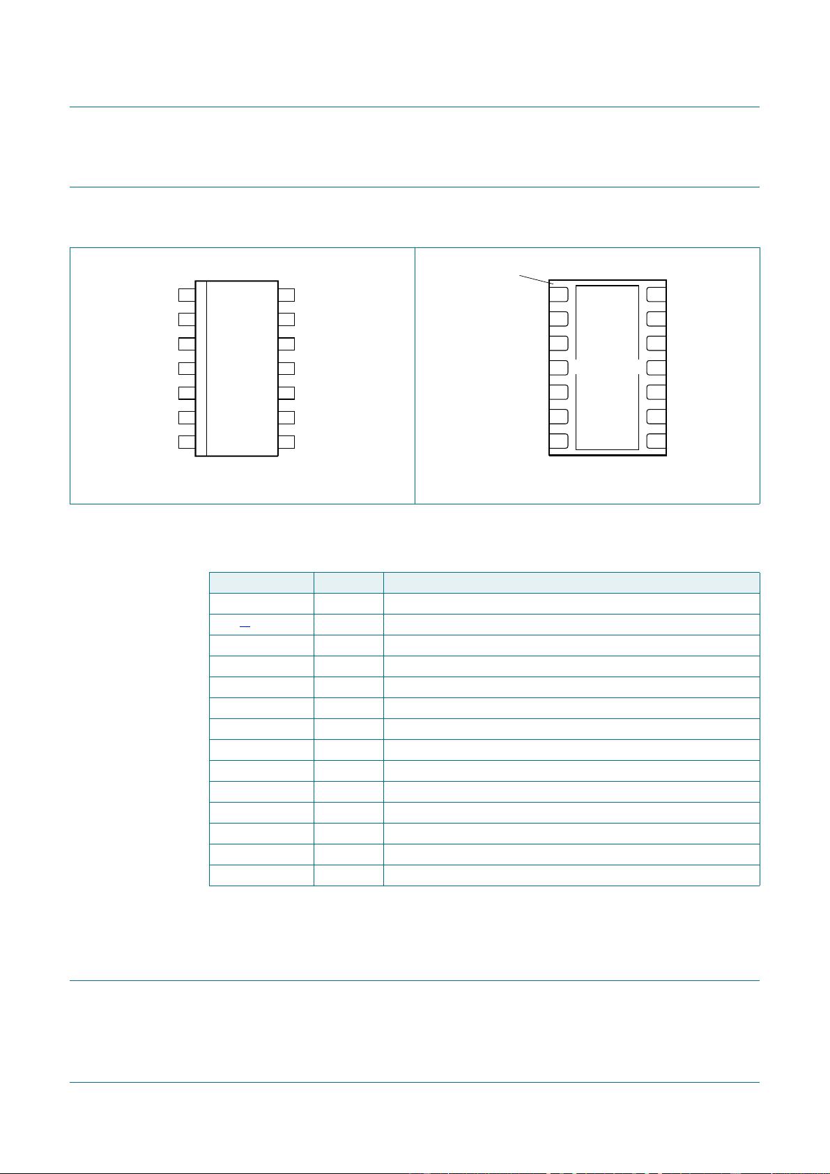
Available in SO14 and HVSON14 packages
TJA1043
High-speed CAN transceiver
Rev. 6 — 10 November 2017 Product data sheet

TJA1043 All information provided in this document is subject to legal disclaimers. © NXP Semiconductors N.V. 2017. All rights reserved.
Product data sheet Rev. 6 — 10 November 2017 2 of 32
NXP Semiconductors
TJA1043
High-speed CAN transceiver
Leadless HVSON14 package (3.0 mm 4.5 mm) with improved Automated Optical
Inspection (AOI) capability
AEC-Q100 qualified
Dark green product (halogen free and Restriction of Hazardous Substances (RoHS)
compliant)
2.2 Low-power management
Very low current Standby and Sleep modes, with local and remote wake-up
Capability to power down the entire node while supporting local, remote and host
wake-up
Wake-up source recognition
Transceiver disengages from the bus (zero load) when V
BAT
absent
Functional behavior predictable under all supply conditions
2.3 Protection and diagnosis (detection and signalling)
High ESD handling capability on the bus pins
Bus pins and V
BAT
protected against transients in automotive environments
Transmit Data (TXD) dominant time-out function with diagnosis
TXD-to-RXD short-circuit handler with diagnosis
Thermal protection with diagnosis
Undervoltage detection and recovery on pins V
CC
, V
IO
and V
BAT
Bus line short-circuit diagnosis
Bus dominant clamping diagnosis
Cold start diagnosis (first battery connection)
3. Quick reference data
Table 1. Quick reference data
Symbol Parameter Conditions Min Typ Max Unit
V
CC
supply voltage 4.5 - 5.5 V
V
IO
supply voltage on pin V
IO
2.8 - 5.5 V
V
uvd(VCC)
undervoltage detection voltage on
pin V
CC
33.54.3V
V
uvd(VIO)
undervoltage detection voltage on
pin V
IO
V
BAT
or V
CC
> 4.5 V 0.8 1.8 2.5 V
I
CC
supply current Normal mode; bus dominant 30 48 65 mA
Normal or Listen-only mode; bus recessive 3 6 9 mA
Standby or Sleep mode 0 0.75 2 A
I
IO
supply current on pin V
IO
Normal mode; V
TXD
= 0 V (dominant) - 150 500 A
Normal or Listen-only mode; V
TXD
=V
IO
(recessive)
014 A
Standby or Sleep mode 0 1 4 A
V
ESD
electrostatic discharge voltage IEC 61000-4-2 at pins CANH and CANL 8- +8kV

TJA1043 All information provided in this document is subject to legal disclaimers. © NXP Semiconductors N.V. 2017. All rights reserved.
Product data sheet Rev. 6 — 10 November 2017 3 of 32
NXP Semiconductors
TJA1043
High-speed CAN transceiver
4. Ordering information
V
CANH
voltage on pin CANH 58 - +58 V
V
CANL
voltage on pin CANL 58 - +58 V
T
vj
virtual junction temperature 40 - +150 C
Table 1. Quick reference data
…continued
Symbol Parameter Conditions Min Typ Max Unit
Table 2. Ordering information
Type number Package
Name Description Version
TJA1043T SO14 plastic small outline package; 14 leads; body width 3.9 mm SOT108-1
TJA1043TK HVSON14 plastic, thermal enhanced very thin small outline package; no leads;
14 terminals; body 3 4.5 0.85 mm
SOT1086-2

TJA1043 All information provided in this document is subject to legal disclaimers. © NXP Semiconductors N.V. 2017. All rights reserved.
Product data sheet Rev. 6 — 10 November 2017 4 of 32
NXP Semiconductors
TJA1043
High-speed CAN transceiver
5. Block diagram
Fig 1. Block diagram
7(03(5$785(
3527(&7,21
7,0(287
02'(
&21752/
:$.(83
&21752/
(5525
'(7(&7,21
08;
'5,9(5
7;'
9
,2
5;'
6/23(
&21752/
'5,9(5
9
&&
&$1+
&$1/
*1'
7-$
63/,7
63/,7
:$.(83
),/7(5
DDD
9
&&
9
,2
9
%$7
67%B1
(1
(55B1
9
%$7
:$.(
9
%$7
,1+

TJA1043 All information provided in this document is subject to legal disclaimers. © NXP Semiconductors N.V. 2017. All rights reserved.
Product data sheet Rev. 6 — 10 November 2017 5 of 32
NXP Semiconductors
TJA1043
High-speed CAN transceiver
6. Pinning information
6.1 Pinning
6.2 Pin description
[1] HVSON14 package die supply ground is connected to both the GND pin and the exposed center pad. The
GND pin must be soldered to board ground. For enhanced thermal and electrical performance, it is
recommended that the exposed center pad also be soldered to board ground.
7. Functional description
The TJA1043 is a stand-alone high-speed CAN transceiver with a number of operating
modes, fail-safe features and diagnostic features that offer enhanced system reliability
and advanced power management. The transceiver combines the functionality of the
Fig 2. Pin configuration diagram: SO14 Fig 3. Pin configuration diagram: HVSON14
7-$7
7;' 67%B1
*1' &$1+
9
&&
&$1/
5;' 63/,7
9
,2
9
%$7
(1 :$.(
,1+ (55B1
DDD
WHUPLQDO
LQGH[DUHD
7-$7.
7;'
*1'
5;'
9
,2
(1
,1+
67%B1
&$1+
&$1/
63/,7
9
%$7
:$.(
(55B1
9
&&
DDD
Table 3. Pin description
Symbol Pin Description
TXD 1 transmit data input
GND
[1]
2 ground supply
V
CC
3 transceiver supply voltage
RXD 4 receive data output; reads out data from the bus lines
V
IO
5 supply voltage for I/O level adaptor
EN 6 enable control input
INH 7 inhibit output for switching external voltage regulators
ERR_N 8 error and power-on indication output (active LOW)
WAKE 9 local wake-up input
V
BAT
10 battery supply voltage
SPLIT 11 common-mode stabilization output
CANL 12 LOW-level CAN bus line
CANH 13 HIGH-level CAN bus line
STB_N 14 standby control input (active LOW)
剩余31页未读,继续阅读


安全验证
文档复制为VIP权益,开通VIP直接复制

评论0