
- 12 -
datasheetK4B4G1646E DDR3L SDRAM
Rev. 1.1
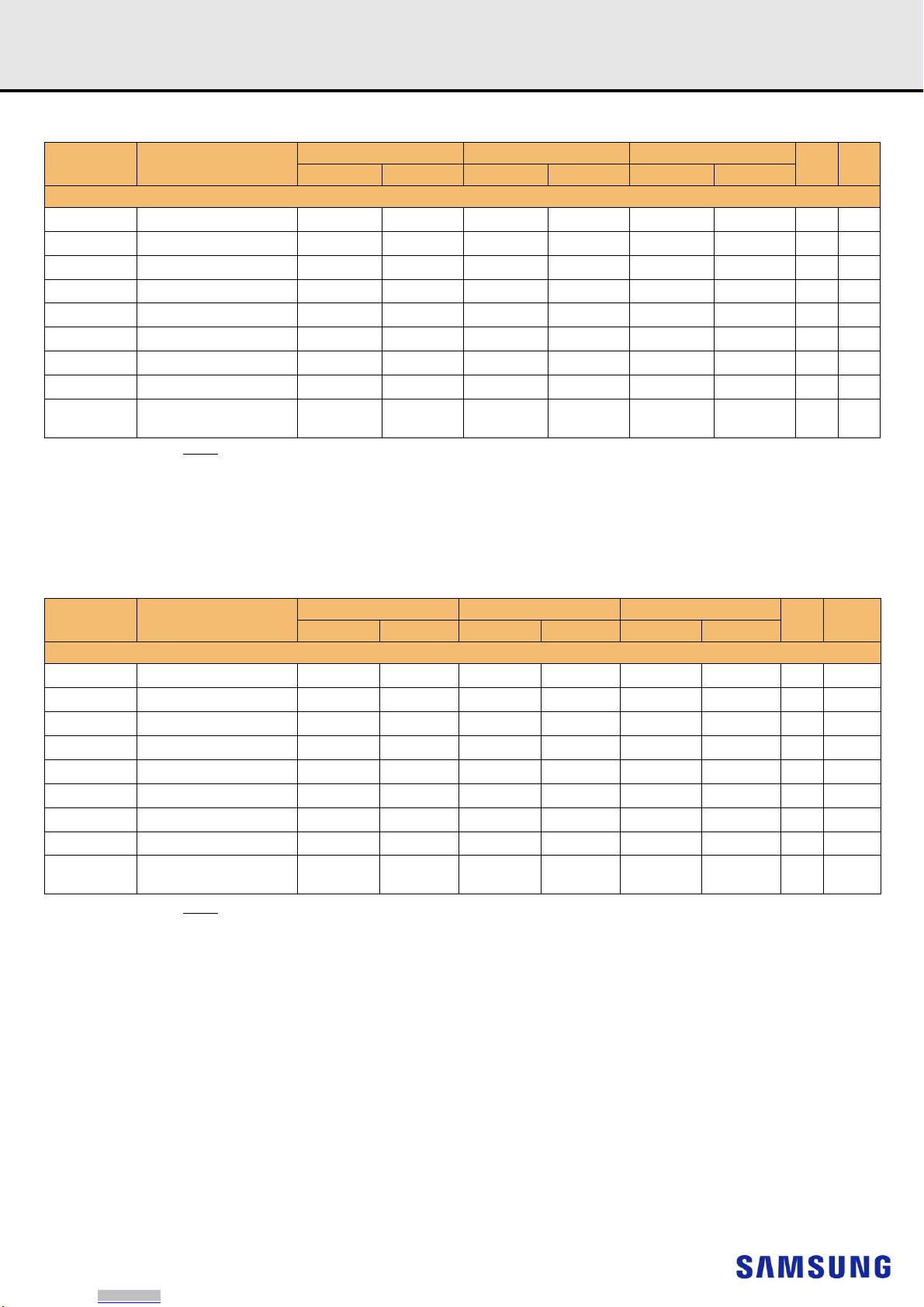
[ Table 9 ] Single-ended AC & DC input levels for DQ and DM (1.35V)
NOTE :
1. For input only pins except RESET
, V
REF
= V
REFDQ
(DC)
2.See "Overshoot and Undershoot specifications" section.
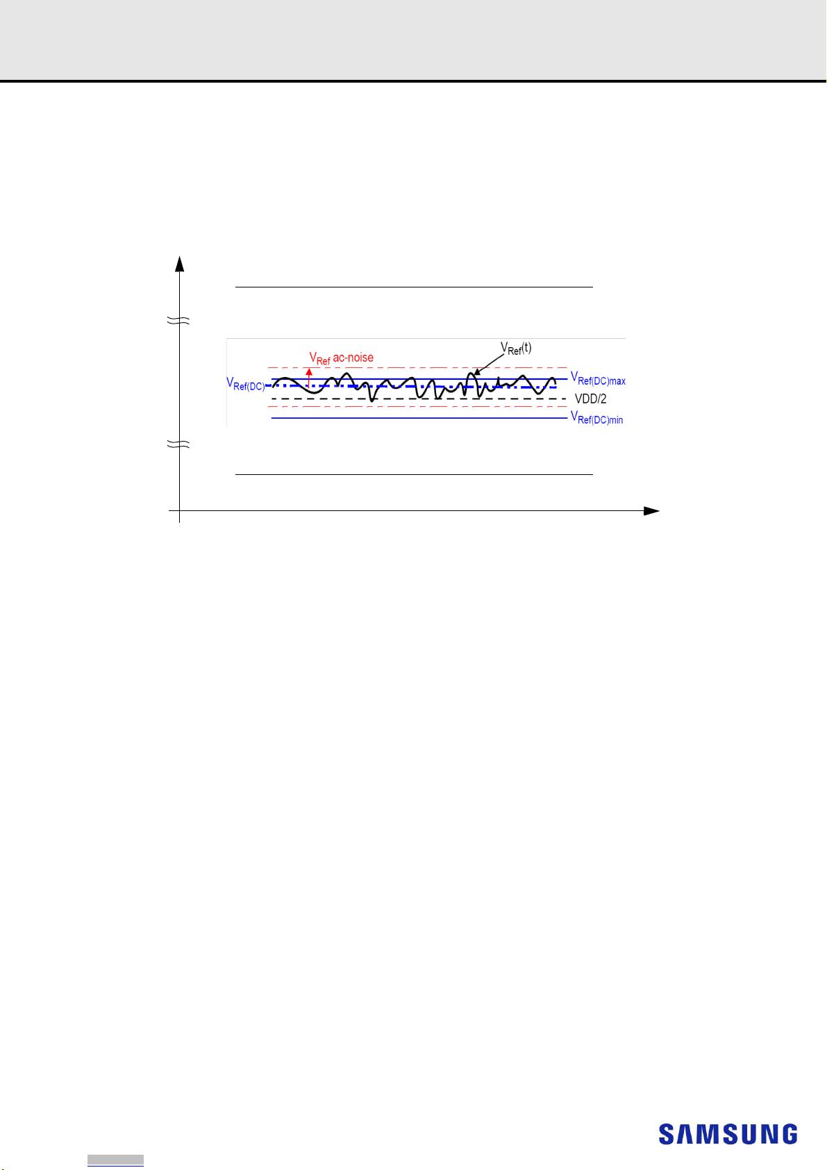
3. The ac peak noise on VRef may not allow VRef to deviate from VRefDQ(DC) by more than +/-1% VDD (for reference: approx. +/- 13.5 mV).
4. For reference: approx. VDD/2 +/- 13.5 mV.
5. These levels apply for 1.35 Volt operation only. If the device is operated at 1.5 V, the respective levels in JESD79-3 ( VIH/L.DQ(DC100), VIH/L.DQ(AC175), VIH/
L.DQ(AC150), VIH/L.DQ(AC135), etc. ) apply. The 1.5 V levels (VIH/L.DQ(DC100), VIH/L.DQ(AC175), VIH/L.DQ(AC150), VIH/L.DQ(AC135), etc. ) do not apply when the
device is operated in the 1.35 voltage range.
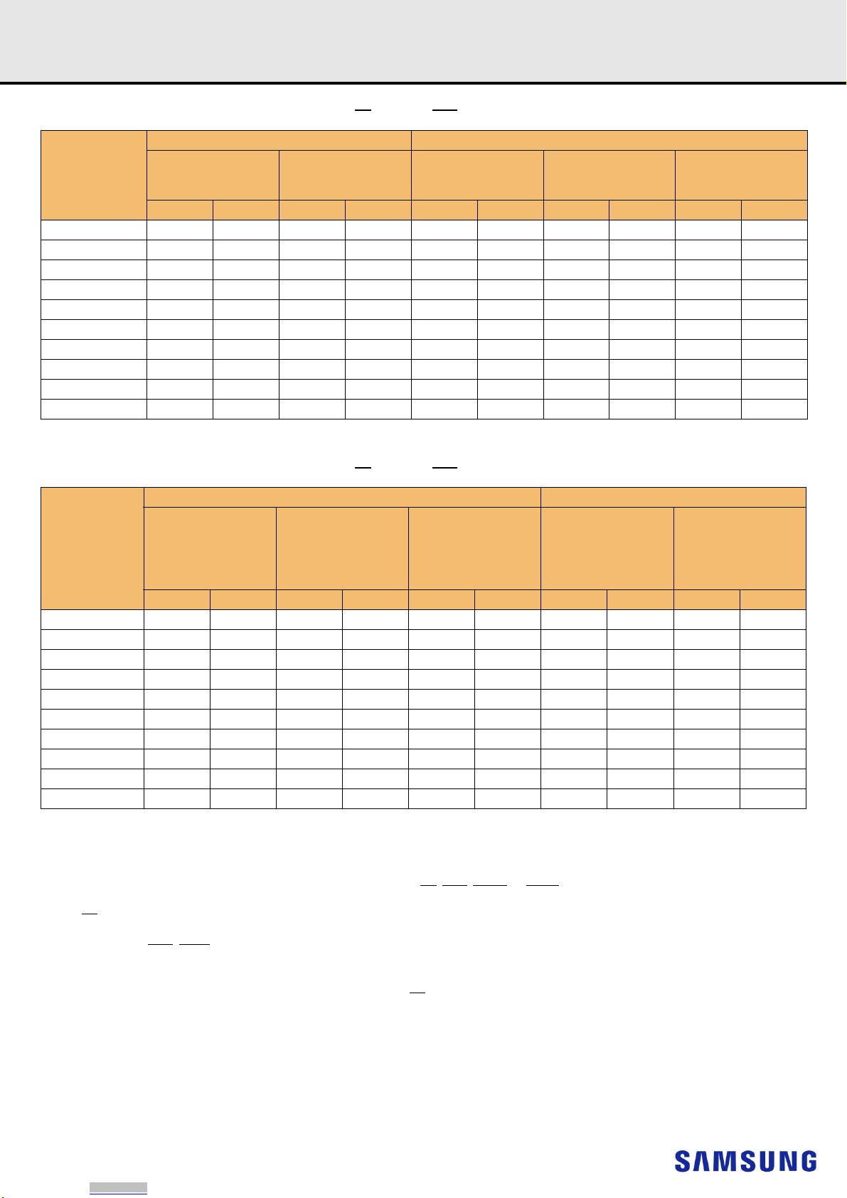
[ Table 10 ] Single-ended AC & DC input levels for DQ and DM (1.5V)
NOTE :
1. For input only pins except RESET
, V
REF
= V
REFDQ
(DC)
2.See "Overshoot and Undershoot specifications" section.
3. The ac peak noise on VRef may not allow VRef to deviate from VRefDQ(DC) by more than +/-1% VDD (for reference: approx. +/- 15 mV).
4. For reference: approx. VDD/2 +/- 15 mV.
5. VIH(dc) is used as a simplified symbol for VIH.DQ(DC100)
6. VIL(dc) is used as a simplified symbol for VIL.DQ(DC100)
7. VIH(ac) is used as a simplified symbol for VIH.DQ(AC175), VIH.DQ(AC150), and VIH.DQ(AC135); VIH.DQ(AC175) value is used when Vref + 0.175V is referenced,
VIH.DQ(AC150) value is used when Vref + 0.150V is referenced, and VIH.DQ(AC135) value is used when Vref + 0.135V is referenced.
8. VIL(ac) is used as a simplified symbol for VIL.DQ(AC175), VIL.DQ(AC150), and VIL.DQ(AC135); VIL.DQ(AC175) value is used when Vref - 0.175V is referenced,
VIL.DQ(AC150) value is used when Vref - 0.150V is referenced, and VIL.DQ(AC135) value is used when Vref - 0.135V is referenced.
9. V
REF
DQ
(DC) is measured relative to VDD at the same point in time on the same device
10. Optional in DDR3 SDRAM for DDR3-800/1066/1333/1600: Users should refer to the DRAM supplier data sheetand/or the DIMM SPD to determine if DDR3 SDRAM devices
support this option.
Symbol Parameter
DDR3L-800/1066 DDR3L-1333/1600 DDR3L-1866
Unit NOTE
Min. Max. Min. Max. Min. Max.
1.35V
V
IH.DQ
(DC90)
DC input logic high
V
REF
+ 90 V
DD
V
REF
+ 90 V
DD
V
REF
+ 90 V
DD
mV 1
V
IL.DQ
(DC90)
DC input logic low
V
SS
V
REF
- 90 V
SS
V
REF
- 90 V
SS
V
REF
- 90
mV 1
V
IH.DQ
(AC160)
AC input logic high
V
REF
+ 160
Note 2----mV1,2,5
V
IL.DQ
(AC160)
AC input logic low Note 2
V
REF
- 160
----mV1,2,5
V
IH.DQ
(AC135)
AC input logic high
V
REF
+ 135
Note 2
V
REF
+ 135
Note 2 - - mV 1,2,5
V
IL.DQ
(AC135)
AC input logic low Note 2
V
REF
- 135
Note 2
V
REF
- 135
- - mV 1,2,5
V
IH.DQ
(AC130)
AC input logic high ----
V
REF
+ 130
Note 2 mV 1,2,5
V
IL.DQ
(AC130)
AC input logic low ----Note 2
V
REF
- 130
mV 1,2,5
V
REF
DQ
(DC)
Reference Voltage for DQ,
DM inputs
0.49*V
DD
0.51*V
DD
0.49*V
DD
0.51*V
DD
0.49*V
DD
0.51*V
DD
V3,4
Symbol Parameter
DDR3-800/1066 DDR3-1333/1600 DDR3-1866
Unit NOTE
Min. Max. Min. Max. Min. Max.
1.5V
V
IH.DQ
(DC100)
DC input logic high
V
REF
+ 100 V
DD
V
REF
+ 100 V
DD
V
REF
+ 100 V
DD
mV 1,5
V
IL.DQ
(DC100)
DC input logic low
V
SS
V
REF
- 100 V
SS
V
REF
- 100 V
SS
V
REF
- 100
mV 1,6
V
IH.DQ
(AC175)
AC input logic high
V
REF
+ 175
NOTE 2 - - - - mV 1,2,7
V
IL.DQ
(AC175)
AC input logic low NOTE 2
V
REF
- 175
----mV1,2,8
V
IH.DQ
(AC150)
AC input logic high
V
REF
+ 150
NOTE 2
V
REF
+ 150
NOTE 2 - - mV 1,2,7
V
IL.DQ
(AC150)
AC input logic low NOTE 2
V
REF
- 150
NOTE 2
V
REF
- 150
- - mV 1,2,8
V
IH.DQ
(AC135)
AC input logic high
V
REF
+ 135
NOTE 2
V
REF
+ 135
NOTE 2
V
REF
+ 135
NOTE 2 mV 1,2,7,10
V
IL.DQ
(AC135)
AC input logic low NOTE 2
V
REF
- 135
NOTE 2
V
REF
- 135
NOTE 2
V
REF
- 135
mV 1,2,8,10
V
REF
DQ
(DC)
Reference Voltage for DQ,
DM inputs
0.49*V
DD
0.51*V
DD
0.49*V
DD
0.51*V
DD
0.49*V
DD
0.51*V
DD
V3,4,9
Downloaded from Arrow.com.Downloaded from Arrow.com.Downloaded from Arrow.com.Downloaded from Arrow.com.Downloaded from Arrow.com.Downloaded from Arrow.com.Downloaded from Arrow.com.Downloaded from Arrow.com.Downloaded from Arrow.com.Downloaded from Arrow.com.Downloaded from Arrow.com.Downloaded from Arrow.com.

剩余70页未读,继续阅读


