"TUSB2E11 USB 2.0-eUSB2 中继器1 特性详解"
需积分: 9 11 浏览量
更新于2024-01-14
4
收藏 1.95MB PDF 举报
TI-TUSB2E11.pdf 是一个 USB 2.0-eUSB2 中继器的规格说明书,主要介绍了该中继器的特性。该中继器具有USB 2.0和eUSB2(1.2 版)兼容性,支持低速、全速、高速信号以及20ps卓越高速总抖动。此外,它还具有寄存器访问协议接收器功能,支持主机和器件模式(双重角色器件)。中继器还能自动检测I2C或自举引脚选项,并支持多种配置。器件变体包括eUSB2 1.0V 或 1.2V 信令接口,适用于不同产品外形尺寸的eUSB2布线损耗补偿水平,以及1.2V 或 1.8V I2C 接口。此外,该中继器还支持可选电池充电和检测,BC 1.2 CDP 或 DCP 分频器模式广播,数据感知 USB Type-C™ 兼容 BC 1.2 SDP、CDP 和 DCP 分频器模式检测,充电器广播或检测之间的双重角色自动切换,以及支持CTA-936 USB Carkit UART。此外,该中继器还支持自动恢复 ECR 以及 L2 中断恢复模式,可选GPIO:中断 GPIO2、调试、I2C ↔ GPIO0/1,以及I2C 可访问调试功能适用于制造测试。该中继器广泛应用于笔记本电脑和台式机、手机、平板电脑、可穿戴设备以及便携式电子产品等领域。
TI-TUSB2E11.pdf 文件提供了关于TUSB2E11 USB 2.0-eUSB2中继器的详细规格和特性介绍。本文介绍了该中继器的兼容性、信号支持能力、高速总抖动性能、I2C或自举引脚选项、器件变体、电池充电和检测功能、CTA-936 USB Carkit UART支持、自动恢复和中断恢复模式、以及可选GPIO等功能。该中继器适用于多种电子设备,并具有广泛的应用前景。
综上所述,TI-TUSB2E11.pdf文件详细介绍了TUSB2E11 USB 2.0-eUSB2中继器的特性和功能,为用户提供了全面的规格说明和硬件参数,有助于用户了解和选用适合自己产品的中继器。

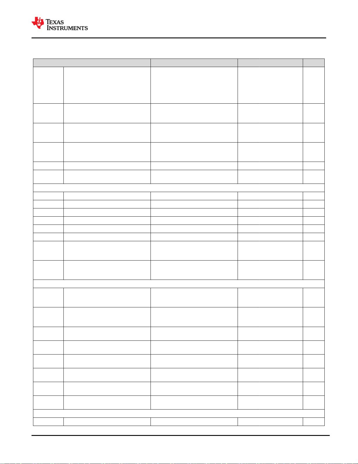
7.4 Thermal Information
THERMAL METRIC
(1)
TUSB2E11
UNITYCG (DSBGA)
15 PINS
R
θJA
Junction-to-ambient thermal resistance 90.5 °C/W
R
θJC(top)
Junction-to-case (top) thermal resistance 0.6 °C/W
R
θJB
Junction-to-board thermal resistance 22.9 °C/W
Ψ
JT
Junction-to-top characterization parameter 0.4 °C/W
Ψ
JB
Junction-to-board characterization parameter 22.9 °C/W
(1) For more information about traditional and new thermal metrics, see the Semiconductor and IC Package Thermal Metrics application
report.
7.5 Electrical Characteristics
over operating free-air temperature range (unless otherwise noted)
PARAMETER TEST CONDITIONS MIN TYP MAX UNIT
POWER
P
WC_1V8
Absolute worst case peak power
consumption (VDD1V8 only) for power
supply budgeting
I2C interface active, GPIOs in output
mode, repeater in HS mode with USB
transmitting, maximum RX EQ, max TX
VOD and PE settings, maximum
transition density. T
A
= −20°C to 85°C.
280 mW
P
WC_3V3
Absolute worst case peak power
consumption (VDD3V3 only) for power
supply budgeting
I2C interface active, GPIOs in output
mode, repeater in HS mode with USB
transmitting, maximum RX EQ, max TX
VOD and PE settings, maximum
transition density. T
A
= –20°C to 85°C.
30 mW
P
WCFS_3V3
Absolute worst case peak power
consumption (VDD3V3 only) for power
supply budgeting
I2C interface active, GPIOs in output
mode, repeater in FS mode with USB
Asynchronous traffic. T
A
= –20°C to
85°C.
75 mW
P
HS_IOC
USB Audio ISOC High-speed
Maximum TX Vod/Maximum TX PE for
both USB and eUSB2. Averaged over 8
ms and only 1 uFrame with data packet.
Toff threshold = 1/32. Host Peripheral
Mode.
35 mW
P
PD
Powered down
Device powered, RESETB=Low,
T
A
=25°C, (DP/DN Voltage ≤ VDD3V3).
9 µW
P
Disabled
Disabled
Device powered, I2C/GPIO interfaces
functional but idle, repeater is disabled
and put into the lowest power state and
non-functional. T
A
=25°C, (DP/DN
Voltage ≤ VDD3V3).
43 95 µW
P
Detach
USB unconnected
I2C/GPIO interfaces idle, repeater is
connected to a eUSB2 PHY and waiting
for a USB attach event. T
A
= 25°C,
(DP/DN Voltage ≤ VDD3V3)
43 85 µW
P
Suspend
L2 Suspend (host mode)
I2C/GPIO interfaces idle, USB link is in
L2, repeater is monitoring for a resume/
remote wake event. T
A
= 25°C, (DP/DN
Voltage ≤ VDD3V3). In peripheral mode
additional current is present due the DP
pull up.
45 85 µW
TUSB2E11
ZHCSQH7A – NOVEMBER 2021 – REVISED JUNE 2022
www.ti.com.cn
10 Submit Document Feedback
Copyright © 2022 Texas Instruments Incorporated
Product Folder Links: TUSB2E11

剩余55页未读,继续阅读
点击了解资源详情
点击了解资源详情
点击了解资源详情
2022-12-03 上传
2022-10-28 上传
2022-10-28 上传
2022-10-28 上传
104 浏览量
2022-12-03 上传

不觉明了
- 粉丝: 7352
- 资源: 5764
 我的内容管理
展开
我的内容管理
展开


最新资源
- robot_joint.tar.gz
- MT8-RGB程序更新 .zip
- Debouncer:Arduino的反跳库
- torch_sparse-0.6.4-cp36-cp36m-win_amd64whl.zip
- CourseSystem:C# 窗体应用程序,课程教务系统
- ngtrongtrung.github.io
- C20
- 技嘉B365M+9100F+5700XT(讯景雪狼版)
- flipendo-website:Flipendo 网站
- 智睿中小学校网站系统官方版源码 v3.3.0
- torch_sparse-0.6.7-cp37-cp37m-linux_x86_64whl.zip
- 取GB2312汉字.rar
- 纯CSS绿色下划线焦点的简洁导航
- 点文件:我的点文件
- fractals_py_p5:画出精美图片和曲线的五种方法称为分形
- 小学生噩梦--口算题卡生成器
