Document Number: 001-98284 Rev. *M Page 20 of 134
3.3.3 Power-On (Cold) Reset
When the core voltage supply remains at or below the V
CC
(low) voltage for t
PD
time, then rises to V
CC (Minimum)
the device will
begin its Power-On Reset (POR) process. POR continues until the end of t
PU
. During t
PU
the device does not react to external input
signals nor drive any outputs. Following the end of t
PU
the device transitions to the Interface Standby state and can accept
commands. For additional information on POR see Power-On (Cold) Reset on page 29.
3.3.4 Hardware (Warm) Reset
Some of the device package options provide a RESET# input. When RESET# is driven low for t
RP
time the device starts the
hardware reset process. The process continues for t
RPH
time. Following the end of both t
RPH
and the reset hold time following the
rise of RESET# (t
RH
) the device transitions to the Interface Standby state and can accept commands. For additional information on
hardware reset see POR followed by Hardware Reset on page 29.
3.3.5 Interface Standby
When CS# is high the SPI interface is in standby state. Inputs other than RESET# are ignored. The interface waits for the beginning
of a new command. The next interface state is Instruction Cycle when CS# goes low to begin a new command.
While in interface standby state the memory device draws standby current (I
SB
) if no embedded algorithm is in progress. If an
embedded algorithm is in progress, the related current is drawn until the end of the algorithm when the entire device returns to
standby current draw.
3.3.6 Instruction Cycle
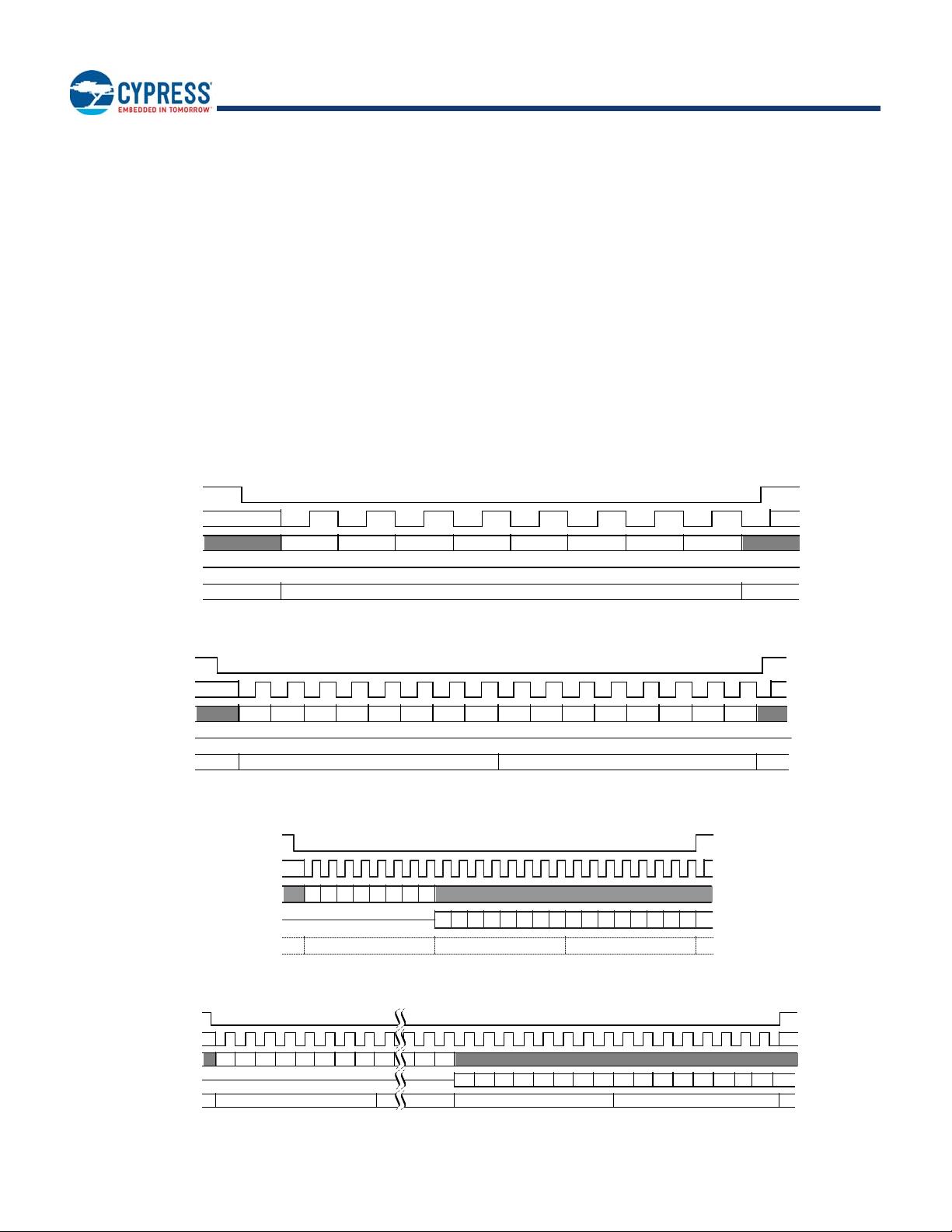
When the host drives the MSB of an instruction and CS# goes low, on the next rising edge of SCK the device captures the MSB of
the instruction that begins the new command. On each following rising edge of SCK the device captures the next lower significance
bit of the 8 bit instruction. The host keeps RESET# high, CS# low, HOLD# high, and drives Write Protect (WP#) signal as needed for
the instruction. However, WP# is only relevant during instruction cycles of a WRR command and is otherwise ignored.
Each instruction selects the address space that is operated on and the transfer format used during the remainder of the command.
The transfer format may be Single, Dual output, Quad output, Dual I/O, Quad I/O, DDR Single I/O, DDR Dual I/O, or DDR Quad I/O.
The expected next interface state depends on the instruction received.
Some commands are stand alone, needing no address or data transfer to or from the memory. The host returns CS# high after the
rising edge of SCK for the eighth bit of the instruction in such commands. The next interface state in this case is Interface Standby.
3.3.7 Hold
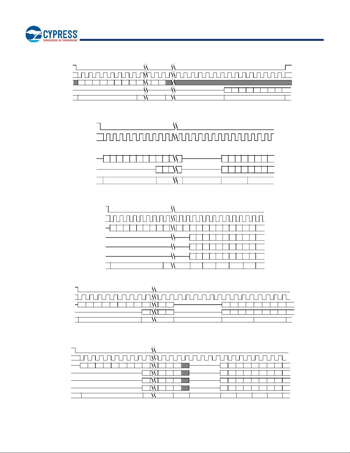
When Quad mode is not enabled (CR[1]=0) the HOLD# / I/O3 signal is used as the HOLD# input. The host keeps RESET# high,
HOLD# low, SCK may be at a valid level or continue toggling, and CS# is low. When HOLD# is low a command is paused, as though
SCK were held low. SI / I/O0 and SO / I/O1 ignore the input level when acting as inputs and are high impedance when acting as
outputs during hold state. Whether these signals are input or output depends on the command and the point in the command
sequence when HOLD# is asserted low.
When HOLD# returns high the next state is the same state the interface was in just before HOLD# was asserted low.
When Quad mode is enabled the HOLD# / I/O3 signal is used as I/O3.
During DDR commands the HOLD# and WP# inputs are ignored.
3.3.8 Single Input Cycle - Host to Memory Transfer
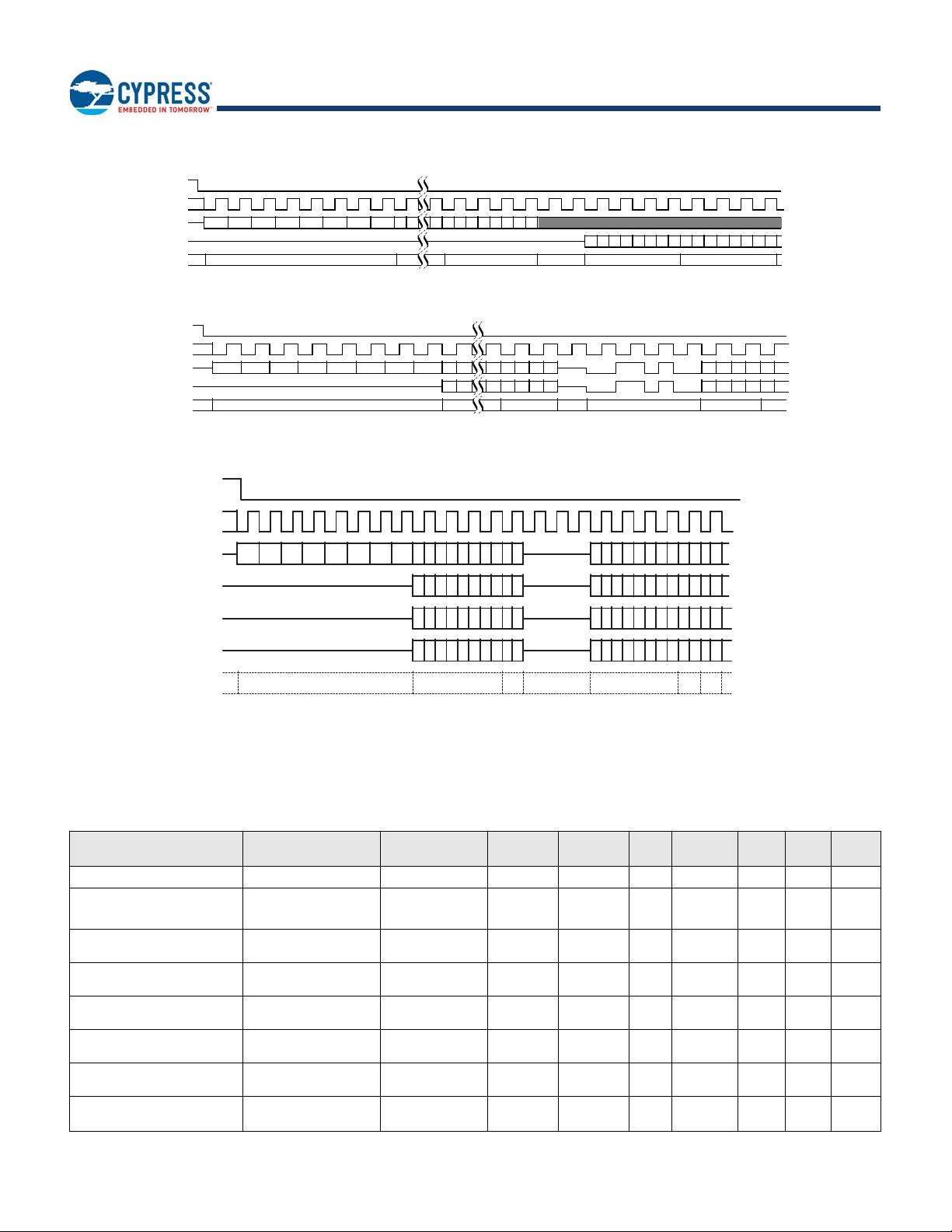
Several commands transfer information after the instruction on the single serial input (SI) signal from host to the memory device. The
dual output, and quad output commands send address to the memory using only SI but return read data using the I/O signals. The
host keeps RESET# high, CS# low, HOLD# high, and drives SI as needed for the command. The memory does not drive the Serial
Output (SO) signal.
The expected next interface state depends on the instruction. Some instructions continue sending address or data to the memory
using additional Single Input Cycles. Others may transition to Single Latency, or directly to Single, Dual, or Quad Output.


