AND9418/D
www.onsemi.com
8
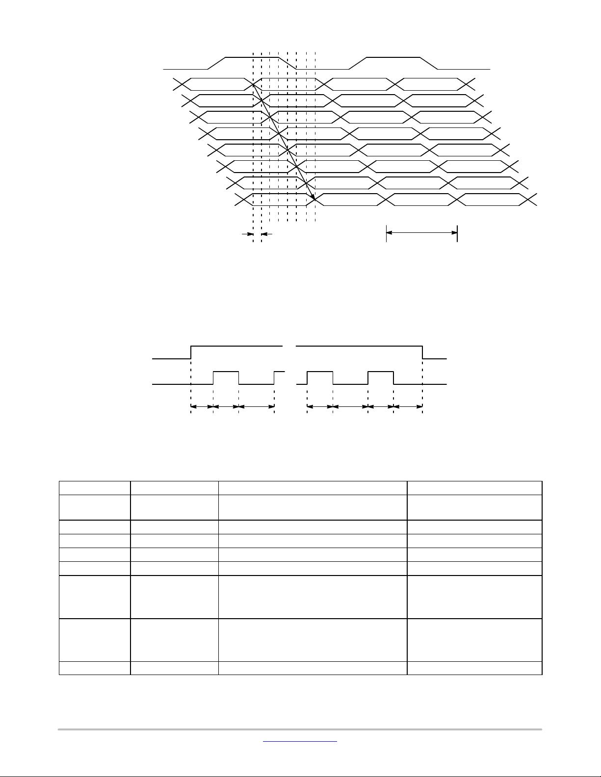
Sensor timing is shown in terms of pixel clock cycles (see
Figure 5). The recommended pixel clock frequency is
74.25 MHz. The vertical blanking and the total frame time
equations assume that the integration time (coarse
integration time plus fine integration time) is less than the
number of active lines plus the blanking lines:
Coarse Integration Time < Window Height + V. Blanking (eq. 1)
If this is not the case, the number of integration lines must
be used instead to determine the frame time, (see Table 3).
In this example, it is assumed that the coarse integration time
control is programmed with 2000 rows and the fine shutter
width total is zero.
For Master mode, if the integration time registers exceed
the total readout time, then the vertical blanking time is
internally extended automatically to adjust for the additional
integration time required. This extended value is not written
back to the frame_length_lines register. The frame_length_
lines register can be used to adjust frame-to-frame readout
time. This register does not affect the exposure time but it
may extend the readout time.
Table 3. FRAME TIME: LONG INTEGRATION TIME
Parameter Name Equation (Number of Pixel Clock Cycles) Default Timing at 74.25 MHz
F’ Total Frame Time
(Long Integration Time)
Context A: (R0x3012 * (A + Q)) − R0x3014 + P1+P2
Context B: (R0x3016 * (A + Q)) − R0x3018 + P1+P2
2,776,012 Pixel Clocks = 37.4 ms
EXPOSURE
Total integration time is the result of coarse_integration_
time and fine_integration_time registers, and depends also
on whether manual or automatic exposure is selected.
The actual total integration time, t
INT
is defined as:
t
INT
+ t
INTCoarse
) t
INTFine
(eq. 2)
= (number of lines of integration * line time) + (number of
pixels of integration * pixel time).
Where:
• Number of Lines of Integration (Auto Exposure
Control: Enabled): When automatic exposure control
(AEC) is enabled, the number of lines of integration
may vary from frame to frame, with the limits
controlled by R0x311E (minimum auto exposure time)
and R0x311C (maximum auto exposure time).
For a specific frame output, the exposure time (in rows)
can be read in R0x30AC. Fine integration time is not
used by the auto exposure function.
• Number of Lines of Integration (Auto Exposure
Control: Disabled):
♦ Context A: the number of lines of integration equals
the value in R0x3012.
♦ Context B: the number of lines of integration equals
the value in R0x3016.
• Number of Pixels of Integration (Auto Exposure
Control: Disabled):
♦ Context A: the number of pixels of integration
equals the value in R0x3014.
♦ Context B: the number of pixels of integration
equals the value in R0x3018.
Maximum value for t
INTFine
is line_length_pck − 1050.
If the exposure time is to be set to approximately 2.22 ms
and default settings are being used (where one row-time
equals 22.22 ms), a value of “100” is entered in R0x3012
(2.22 ms / 22.22 ms = 100). In this mode, only whole
number row-time increments are allowed − no fractional
time increments can be achieved. It may be possible to adjust
the number of horizontal active or blanking pixels to bring
the desired exposure time to a whole number row-time
increment.
The exposure time using the default power up settings of
the sensor can be determined as follows:
exposure_time = coarse_integreation_time row_time (eq. 3)
exposure_time + (100 rows) (22.22 ms) + 2.22 ms (eq. 4)
Typically, the value of the coarse_integration_time
register is limited to the number of lines per frame (which
includes vertical blanking lines), such that the frame rate is
not affected by the integration time.
Row-time Definition
One row-time is equal to the sum of the number of active
pixels (columns) and the number of horizontal blanking
pixels divided by the pixel readout rate:
row_time +
active_pixels + horizontal_blank_pixels
PIXCLK_frequency
(eq. 5)
row_time
default_settings
+
line_length_pck(R0x300C)
PIXCLK_frequency
(eq. 6)
+
1388
74.25 MHz
+ 18.69 ms
Exposure Indicator
The AR0135CS provides an output pin, FLASH, to
indicate when the exposure takes place. When R0x3046[8]is
set, FLASH is HIGH during exposure. By using
R0x3046[7], the polarity of the FLASH pin can be inverted.


