
BE14CH06-Rogers ARI 9 April 2012 13:38
1 mm
100 μm
50 μm
70 μm
300 μm
100 μm
(111) silicon
Bottom silicon
Top silicon
a
Retrieve
Transfer: contact and release
c
5 mm
d b
0.10%
0.08%
0.06%
0.04%
0.02%
0
m
Tr
a
n
s
f
e
r
:
co
n
tact
a
n
d
r
e
l
ea
Anchors
Adhesives
Nano-
membranes
Strain
Figure 1
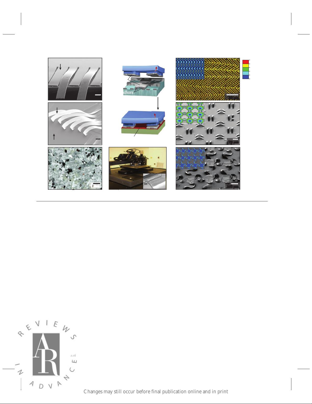
Materials, processing approaches, and layouts that yield stretchable forms of inorganic semiconductors such as silicon and gallium
arsenide. (a) Nanomembranes of these materials, produced from high-quality, single-crystal wafers using lithographic patterning and
etching. (Top) A set of flexible nanomembranes/ribbons (NMs) made of (111) silicon created by anisotropic undercut etching of a
silicon wafer. (Middle) (100) silicon NMs released from a silicon-on-insulator wafer by removal of the buried oxide. (Bottom) A large
collection of GaAs NMs prepared from epitaxial, multilayer stacks of GaAs/AlAs. Selectively etching the sacrificial AlAs layers releases
GaAs NMs. Reproduced with permission from Reference 40. Copyright Nature Publishing Group. (b) Schematic of the process for
transfer printing collections of NMs from their released forms on a source wafer to a target surface. (c) Automatic transfer printing tool.
Inset shows a collection of GaAs NMs printed onto a flexible sheet of polyethylene terephthalate. (d ) Scanning electron microscope
images and (insets) corresponding finite element modeling results for semiconductor NMs bonded to prestrained elastomeric substrates
in three different configurations. Upon releasing the prestrain, controlled buckling processes in the NMs lead to different layouts: (top)
two-dimensional herringbone “wavy” patterns (reproduced with permission from Reference 37, copyright American Chemical Society)
and noncoplanar bridge structures with (middle) straight and (bottom) serpentine (reproduced with permission from Reference 22,
copyright National Academy of Sciences) interconnects. In all cases, strains in the silicon structures themselves are less than ∼0.1%,
even when strains of the overall system exceed 100% in certain configurations.
wafer but tethered at strategic points (i.e., anchors), simply by the action of generalized adhesion
forces to the PDMS, typically dominated by van der Waals interactions (27, 45) (Figure 1b, top).
This transfer can be performed over large areas of uniform or segmented NMs using flat stamps
(27) or over selected areas using structured stamps (46) (Figure 1b, top). The retrieved collections
of NMs (i.e., solid “inks” in this procedure) are selectively delivered to target substrate surfaces,
at predefined locations with microscale precision (Figure 1b, bottom), by printing (39, 47). A
variety of approaches allow the switching in adhesion needed for efficient operation; these range
from rate-dependent viscoelastic effects (27, 48), to biomimetic strategies (45), to use of interfacial
bonding layers (49). Printing with automated tools that include high-resolution cameras for
overlay registration and multidimensional stages for positional control enables submicron scale
116 Kim et al.
Changes may still occur before final publication online and in print
Annu. Rev. Biomed. Eng. 2012.14. Downloaded from www.annualreviews.org
by Cornell University on 06/28/12. For personal use only.
剩余15页未读,继续阅读

墨氲
- 粉丝: 714
- 资源: 8
 我的内容管理
展开
我的内容管理
展开


最新资源
- Lombok 快速入门与注解详解
- SpringSecurity实战:声明式安全控制框架解析
- XML基础教程:从数据传输到存储解析
- Matlab实现图像空间平移与镜像变换示例
- Python流程控制与运算符详解
- Python基础:类型转换与循环语句
- 辰科CD-6024-4控制器说明书:LED亮度调节与触发功能解析
- AE particular插件全面解析:英汉对照与关键参数
- Shell脚本实践:创建tar包、字符串累加与简易运算器
- TMS320F28335:浮点处理器与ADC详解
- 互联网基础与结构解析:从ARPANET到多层次ISP
- Redhat系统中构建与Windows共享的Samba服务器实战
- microPython编程指南:从入门到实践
- 数据结构实验:顺序构建并遍历链表
- NVIDIA TX2系统安装与恢复指南
- C语言实现贪吃蛇游戏基础代码
资源上传下载、课程学习等过程中有任何疑问或建议,欢迎提出宝贵意见哦~我们会及时处理!
点击此处反馈


