
www.ti.com
4 ±1A Single-Supply Low-Side Current Sensing Solution Reference Design TIDU675-June 2015
Copyright © 2015, Texas Instruments Incorporated
2.1 Error Analysis
There are two types of errors introduced by the circuit in Figure 2: offset and gain. To obtain more
information about these types of errors, please refer to TIPD129. Table 2 lists the error sources and their
respective type(s).
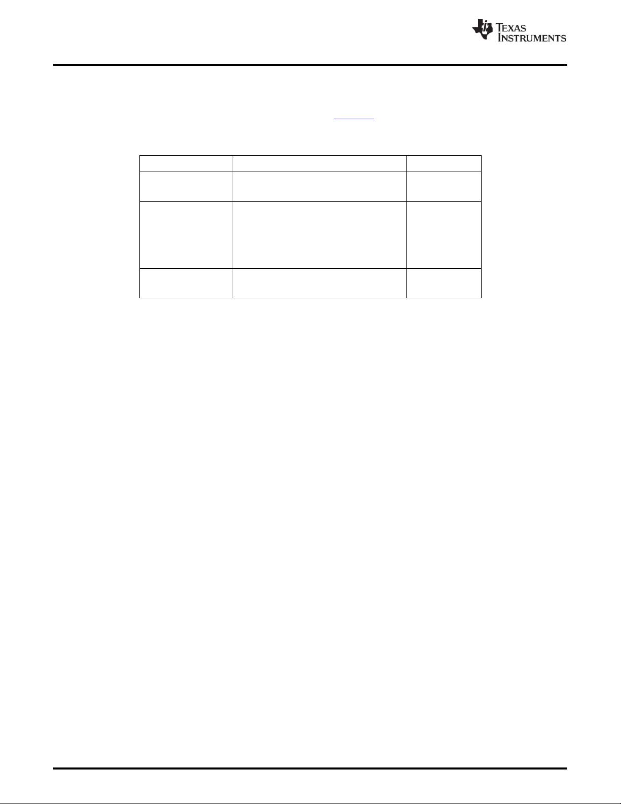
Table 2. Design Error Sources
Error Source
Description
Error Type
Shunt resistor
Shunt resistor tolerance
Gain
Difference Amplifier
U1A and R
1
-R
4
create a difference amplifier.
The ratios of R
2
/R
1
and R
4
/R
3
introduce a gain
error. The absolute value of the ratios
introduce a gain error and the matching of the
ratios determine the CMRR performance,
which translates to an offset error.
Offset & Gain
Reference Voltage
The accuracy of the voltage divider created by
R
5
and R
6
yields an offset error.
Offset
These errors ultimately combine and are measured at the output as gain and offset errors. It is common to
combine them using the root sum squared (RSS) method. This method is used when combining errors
with a normal distribution, thereby yielding typical total error. For a worst-case total error, simply add all
error terms directly.
剩余19页未读,继续阅读


小幽余生不加糖
- 粉丝: 4w+
- 资源: 71
 我的内容管理
收起
我的内容管理
收起
- 我的资源
快来上传第一个资源
 我的收益 登录查看自己的收益
 我的积分
登录查看自己的积分
我的积分
登录查看自己的积分
 我的C币
登录后查看C币余额
我的C币
登录后查看C币余额
 我的收藏
我的收藏  我的下载
我的下载  下载帮助
下载帮助

会员权益专享


最新资源
- 京瓷TASKalfa系列维修手册:安全与操作指南
- 小波变换在视频压缩中的应用
- Microsoft OfficeXP详解:WordXP、ExcelXP和PowerPointXP
- 雀巢在线媒介投放策划:门户网站与广告效果分析
- 用友NC-V56供应链功能升级详解(84页)
- 计算机病毒与防御策略探索
- 企业网NAT技术实践:2022年部署互联网出口策略
- 软件测试面试必备:概念、原则与常见问题解析
- 2022年Windows IIS服务器内外网配置详解与Serv-U FTP服务器安装
- 中国联通:企业级ICT转型与创新实践
- C#图形图像编程深入解析:GDI+与多媒体应用
- Xilinx AXI Interconnect v2.1用户指南
- DIY编程电缆全攻略:接口类型与自制指南
- 电脑维护与硬盘数据恢复指南
- 计算机网络技术专业剖析:人才培养与改革
- 量化多因子指数增强策略:微观视角的实证分析
资源上传下载、课程学习等过程中有任何疑问或建议,欢迎提出宝贵意见哦~我们会及时处理!
点击此处反馈


