
3610 IEEE TRANSACTIONS ON CIRCUITS AND SYSTEMS–I: REGULAR PAPERS, VOL. 66, NO. 9, SEPTEMBER 2019
A Fast-Transient-Response Fully-Integrated Digital
LDO With Adaptive Current Step Size Control
Guigang Cai , Student Member, IEEE, Chenchang Zhan , Member, IEEE,
and Yan Lu , Senior Member, IEEE
Abstract— A 0.6-V 100-mA fully-integrated digital low-dropout
regulator (DLDO) with adaptive current step size control is
presented in this paper. By dividing the main power PMOSs
into ten blocks with different unit-cell sizes, the proposed DLDO
can turn-on/-off small power PMOSs in light load and large
ones in heavy load conditions. High regulation accuracy in a
wide load range and fast transient response are hence achieved.
In addition, an auxiliary power MOS block, which consists of
both PMOS and NMOS transistors, is adopted to eliminate
the limit cycle oscillation (LCO) in light load condition and
to further accelerate the response speed. The proposed DLDO
is fabricated in a 65-nm low-power CMOS technology with an
active area of 0.17 mm
2
including an on-chip output capacitor
of 1nF. The measured undershoot and overshoot voltages are
only 53 and 37 mV, respectively, when the load current changes
between 0 and 100 mA. The quiescent current is 34.6 µA, while
the maximum current efficiency is 99.96%.
Index Terms— Digital low-dropout regulator (DLDO), adaptive
current step size control, wide load range, fully-integrated, fast
transient response.
I. INTRODUCTION
W
ITH the rapid development of economic growth and
technology, smart phones and wearable equipment with
complex functions are playing a more important role in peo-
ple’s life. Among these portable electric devices that rely heav-
ily on battery-power energy, power management integrated cir-
cuits (PMIC), such as low-dropout regulator (LDO), switching
mode power converter (SMPC) and charge pump (CP), are key
feature functional components. Due to the switching behavior,
the output voltage ripple of the SMPC and CP is large, while
that of LDO is smaller for its continuous modulation. What’s
Manuscript received March 14, 2019; accepted May 14, 2019. Date
of publication June 26, 2019; date of current version August 28, 2019.
This work was supported in part by the National Natural Science Foun-
dation of China (NSFC) under Grant 61604067, in part by SZSTI under
Grant JCYJ20170817112233337 and Grant KQJSCX20180319114406851,
and in part by the Research Committee of the University of Macau under
Grant MYRG2018-00102-AMSV. This paper was recommended by Associate
Editor F. Neri. (Corresponding authors: Chenchang Zhan; Yan Lu.)
G. Cai is with the Department of Electrical and Electronic Engineering,
Southern University of Science and Technology, Shenzhen 518055, China, and
also with the State Key Laboratory of Analog and Mixed-Signal VLSI, Uni-
versity of Macau, Macau 999078, China (e-mail: caigg@mail.sustech.edu.cn).
C. Zhan is with the Department of Electrical and Electronic Engineering,
Southern University of Science and Technology, Shenzhen 518055, China
(e-mail: zhancc@sustech.edu.cn).
Y. Lu is with the State Key Laboratory of Analog and Mixed-Signal VLSI,
University of Macau, Macau 999078, China (e-mail: yanlu@um.edu.mo).
Color versions of one or more of the figures in this article are available
online at http://ieeexplore.ieee.org.
Digital Object Identifier 10.1109/TCSI.2019.2917558
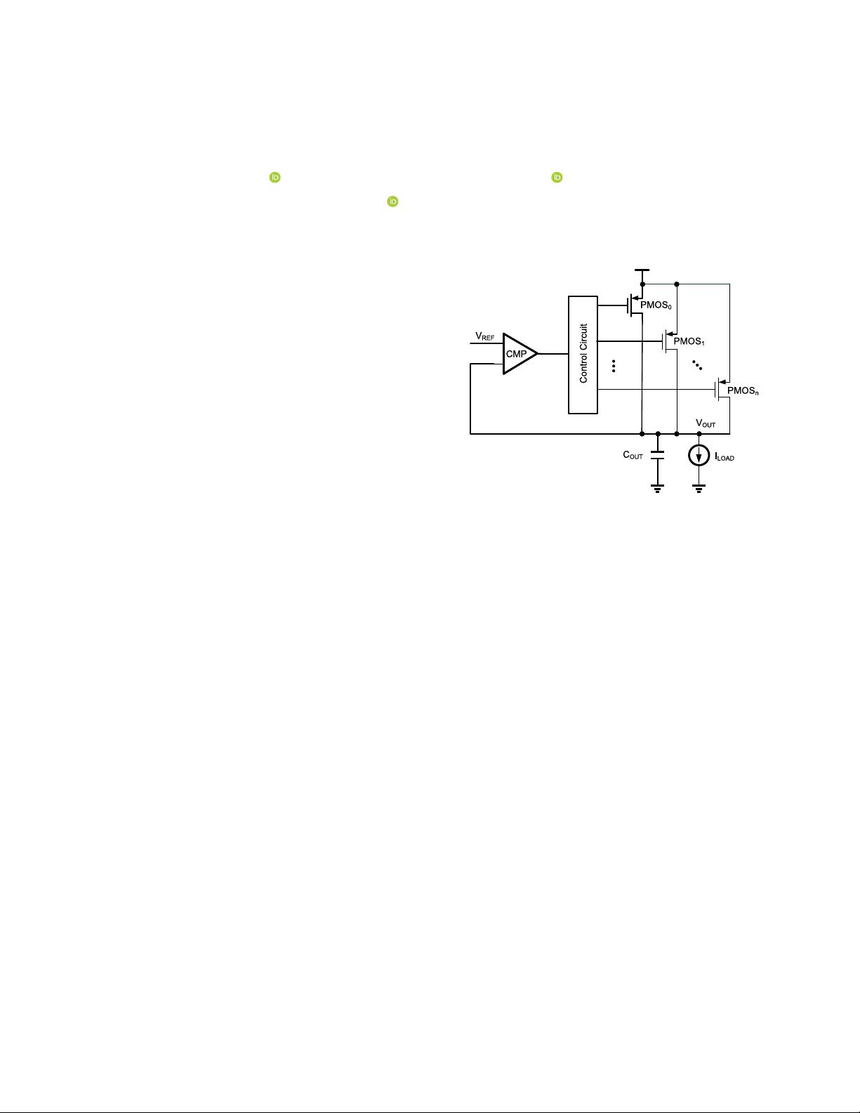
Fig. 1. Block diagram of a generic DLDO.
more, LDO achieves faster transient response, requires less
off-chip component thus less cost compared with SMPC and
CP, which makes it the most frequently used power con-
verter [1]–[5]. In recent years, in order to prolong the working
hours of these portable electric devices, the supply voltage of
some digital blocks has been designed to near/subthreshold
voltage to reduce power consumption, especially in standby
mode. In such a scenario, the traditional analog LDO (ALDO)
consists of analog control loop no longer work effectively.
Therefore, digital LDO (DLDO) was proposed to be an
alternative solution [6].
As shown in Fig. 1, a generic DLDO incorporates with a
comparator CMP, a control circuit which usually consists of
a bidirectional shift register (S/R), a power PMOS array and
an output capacitor C
OUT
. The comparator CMP compares the
difference between the output voltage V
OUT
and the reference
voltage V
REF
then outputs control signal to control circuit,
then a power PMOS will be turned on/off to modulate V
OUT
close to V
REF
. Since only one PMOS is turn on/off each
clock cycle for the S/R operation, the transient speed depends
heavily on the clock frequency. A low clock frequency leads
to small quiescent current I
Q
but slow transient speed. On the
other hand, a high clock frequency results in fast transient
speed but large quiescent current. Furthermore, a too high
clock frequency might cause stability problem and steady-
state limit cycle oscillation (LCO) in no load or light load
condition. The contradiction between regulate accuracy and
the load current range and the regulate speed is another issue
1549-8328 © 2019 IEEE. Personal use is permitted, but republication/redistribution requires IEEE permission.
See http://www.ieee.org/publications_standards/publications/rights/index.html for more information.
下载后可阅读完整内容,剩余9页未读,立即下载

weixin_38665490
- 粉丝: 4
- 资源: 985
 我的内容管理
展开
我的内容管理
展开


最新资源
- 十种常见电感线圈电感量计算公式详解
- 军用车辆:CAN总线的集成与优势
- CAN总线在汽车智能换档系统中的作用与实现
- CAN总线数据超载问题及解决策略
- 汽车车身系统CAN总线设计与应用
- SAP企业需求深度剖析:财务会计与供应链的关键流程与改进策略
- CAN总线在发动机电控系统中的通信设计实践
- Spring与iBATIS整合:快速开发与比较分析
- CAN总线驱动的整车管理系统硬件设计详解
- CAN总线通讯智能节点设计与实现
- DSP实现电动汽车CAN总线通讯技术
- CAN协议网关设计:自动位速率检测与互连
- Xcode免证书调试iPad程序开发指南
- 分布式数据库查询优化算法探讨
- Win7安装VC++6.0完全指南:解决兼容性与Office冲突
- MFC实现学生信息管理系统:登录与数据库操作
资源上传下载、课程学习等过程中有任何疑问或建议,欢迎提出宝贵意见哦~我们会及时处理!
点击此处反馈


