
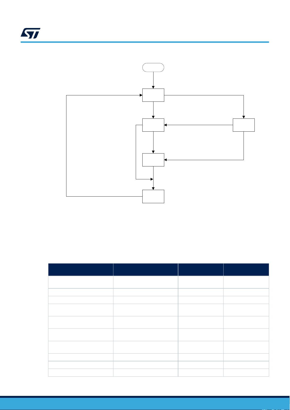
Figure 2. Page status valid transitions
DT45026V1
FORMAT
EEPROM
ERASED
RECEIVE
ACTIVE
VALID
ERASING
Transfer DATA
Write DATA
Write DATA (Page Full)
DATA Transfer to this page completed
(page not full)
DATA transfer to this page completed
(page full)
Erase command issued by application
DATA transfer from this page completed
DATA transfer from this page completed
3.3 Page and variable format
Depending on the STM32 series, flash memory page sizes and composition can vary.
Moreover, for some STM32 series, the EEPROM emulation driver supports either single bank mode, dual bank
mode, or both. The right mode must be selected in the EEPROM emulation driver, according to the mode
supported. See Table 3 for this information.
Table 3. Flash memory properties
STM32 series/value lines Flash memory page sizes
Single bank mode
support
Dual bank mode
support
STM32L4+ series
4 Kbytes (512 words of 64 bits for
DBANK = 1)
No
(1)
Yes
STM32L41x/42x/43x 44x/45x/46x 2 Kbytes (256 words of 64 bits) Yes No
STM32L47x/48x/49x/4Ax 2 Kbytes (256 words of 64 bits) Yes Yes
STM32L552 STM32L562
2 Kbytes (256 words of 64 bits)
(for DBANK = 1)
No
(1)
Yes
STM32G0x0xx and STM32G0x1xx
STM32G0B1xx and STM32G0C1xx
2 Kbytes (256 words of 64 bits) Yes
No
Yes
STM32G4 series
2 Kbytes (256 words of 64 bits)
(for DBANK = 1)
No
(1)
Yes
STM32WB55xx, STM32WB35xx,
STM32WB50CG, STM32WB30CE
4 Kbytes (512 words of 64 bits) Yes No
STM32WL series 2 Kbytes (8 rows of 256 bytes) Yes No
STM32WB15CC, STM32WB10CC 2 Kbytes (256 words of 64 bits) Yes No
STM32U0 series 2 Kbytes (256 words of 64 bits) Yes No
AN4894
Implementing EEPROM emulation
AN4894 - Rev 9
page 6/31

剩余30页未读,继续阅读


atonlink
- 粉丝: 100
- 资源: 7
 我的内容管理
收起
我的内容管理
收起
- 我的资源
快来上传第一个资源
 我的收益 登录查看自己的收益
 我的积分
登录查看自己的积分
我的积分
登录查看自己的积分
 我的C币
登录后查看C币余额
我的C币
登录后查看C币余额
 我的收藏
我的收藏  我的下载
我的下载  下载帮助
下载帮助

会员权益专享


最新资源
- 电力电子系统建模与控制入门
- SQL数据库基础入门:发展历程与关键概念
- DC/DC变换器动态建模与控制方法解析
- 市***专有云IaaS服务:云主机与数据库解决方案
- 紫鸟数据魔方:跨境电商选品神器,助力爆款打造
- 电力电子技术:DC-DC变换器动态模型与控制
- 视觉与实用并重:跨境电商产品开发的六重价值策略
- VB.NET三层架构下的数据库应用程序开发
- 跨境电商产品开发:关键词策略与用户痛点挖掘
- VC-MFC数据库编程技巧与实现
- 亚马逊新品开发策略:选品与市场研究
- 数据库基础知识:从数据到Visual FoxPro应用
- 计算机专业实习经验与项目总结
- Sparkle家族轻量级加密与哈希:提升IoT设备数据安全性
- SQL数据库期末考试精选题与答案解析
- H3C规模数据融合:技术探讨与应用案例解析
资源上传下载、课程学习等过程中有任何疑问或建议,欢迎提出宝贵意见哦~我们会及时处理!
点击此处反馈


