IEEE TRANSACTIONS ON CIRCUITS AND SYSTEMS—II: EXPRESS BRIEFS, VOL. 62, NO. 3, MARCH 2015 241
A Multibit Delta–Sigma Modulator With
Double Noise-Shaped Segmentation
Lin He, Member, IEEE, Guanglong Zhu, Fang Long, Yunchen Zhang, Li Wang,
Fujiang Lin, Senior Member, IEEE, Libin Yao, Senior Member, IEEE, and Xicheng Jiang, Fellow, IEEE
Abstract—This brief proposes a low-power architecture for a
discrete-time (DT) delta–sigma modulator to take full advantages
of increased quantization levels. In the proposed architecture,
noise-shaped segmentation is applied to both the quantizer and the
feedback digital-to-analog converter to maintain a high resolution
and a high linearity and, at the same time, keep the hardware
complexity low. This leads to a significantly reduced output swing
of the integrator to minimize the slewing-related distortion in a
DT implementation. The resulting uniform linear settling behavior
can tolerate a relatively large settling error without degrading the
performance, which greatly relaxes the bandwidth requirement
of the op-amp design. The reduced output swing also allows the
use of low-gain amplifiers, which is particularly attractive for an
advanced technology in which the intrinsic gain of the transistor
is degraded. The proposed architecture is analyzed and verified
through simulation.
Index Terms—Continuous time, delta–sigma (ΔΣ), digital noise
coupling (DNC), discrete time (DT), dynamic element matching
(DEM), low power, low voltage, noise coupling, noise-shaped seg-
mentation, segmentation, segmented quantization, slew, wideband.
I. INTRODUCTION
D
ELTA–SIGMA (ΔΣ) analog-to-digital converters (ADCs)
are the main candidates for high-resolution applications
due to their relative insensitivity to circuit nonidealities. Con-
ventional ΔΣ ADCs are implemented with discrete-time (DT)
loop filters for their highly accurate loop coefficient. Recently,
continuous-time ΔΣ modulators (CTDSMs) [1], [2] based on
RC or Gm-C loop filters have attracted much attention and
nearly dominate the publications in this area, because of their
advantages of high speed, low power, and inherent antialiasing
filtering. However, CTDSMs suffer from clock jitter [3], [4] and
excess loop delay [5], [6], which makes their design much more
complicated than a DT implementation.
There are many ways to reduce the power consumption of a
DT ΔΣ modulator, among which the most straightforward is
to increase the resolution of the multibit quantizer. It reduces
the quantization noise as well as the output signal swings of
the integrators, so that the slew rate and the gain requirement
of the op-amps are relaxed, which is particularly useful for
Manuscript received July 19, 2014; revised September 3, 2014; accepted
November 1, 2014. Date of publication November 7, 2014; date of current ver-
sion March 1, 2015. This work was supported by the National Natural Science
Foundation of China under Project 61204033. This brief was recommended by
Associate Editor P. Rombouts.
L. He, G. Zhu, F. Long, Y. Zhang, L. Wang, and F. Lin are with the Micro-/
Nano-Electronic System Integration Center (MESIC), University of Science
and Technology of China, Hefei 230026, China (e-mail: helin77@ustc.edu.cn).
L. Yao is with Kunming Institute of Physics, Kunming 650223, China.
X. Jiang is with Broadcom Corporation, Irvine, CA 92617 USA.
Digital Object Identifier 10.1109/TCSII.2014.2368261
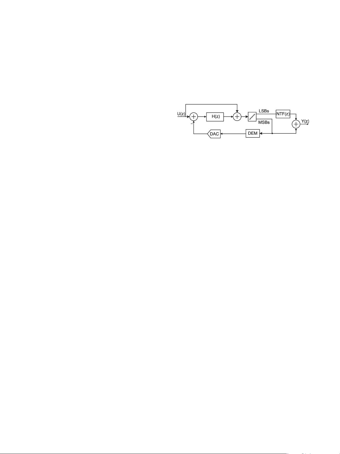
Fig. 1. Leslie–Singh architecture employed in [13].
scaled complementary metal–oxide–semiconductor (CMOS)
technology. Although it looks simple and straightforward, this
strategy faces a practical limitation of the increased complexity
of the dynamic element matching (DEM) logic [7]–[9], which
suffers from an exponential growth problem with the increased
feedback levels.
Attempts have been reported to increase the number of
quantization levels with reasonable hardware complexity, such
as two-step quantizer [10], pipelined quantizer [11], synthetic
aperture radar (SAR) quantizer [12], [13], or nonuniform quan-
tizer [14]. There are also many researches that try to reduce
the complexity of the DEM logic, through the most significant
bit (MSB)-only feedback [13], [15], [16] or digital truncation
[12], [17], [18]. The segmented MSB/least significant bit (LSB)
feedback in a ΔΣ modulator was introduced by Lindfors and
Halonen [19], which is effective in reducing both the step size
at the integrator output as well as the complexity of the DEM
logic. However, the coefficient mismatch between the MSB
digital-to-analog converter (DAC) and the LSB DAC causes a
quantization noise leakage and limits the achievable signal-to-
noise-and-distortion ratio (SNDR).
In this brief, noise-shaped segmentation [20] is applied to
both the quantizer and the feedback DAC to maintain a high
resolution and a linear feedback DAC and, at the same time,
keep the hardware complexity low. This brief is organized
as follows. Section II presents the double noise-shaped
segmentation architecture. Section III analyzes the sensitivity
of the proposed architecture over various circuit nonidealities.
Section IV discusses the implementation issues. Section V
concludes this brief.
II. A
RCHITECTURE
A. Previous Works
It has been demonstrated that, with a segmented quantizer
and MSB-only feedback (see Fig. 1), the complexity of the
DEM logic can be reduced to an acceptable level [13]. This
strategy can be combined with the noise-coupling technique
[21], [22] to minimize the noise leakage problem caused by
1549-7747 © 2014
IEEE. Personal use is permitted, but republication/redistribution requires IEEE permission.
See http://www.ieee.org/publications_standards/publications/rights/index.html for more information.


