
1 Introduction to Hardware Obfuscation: Motivation … 5
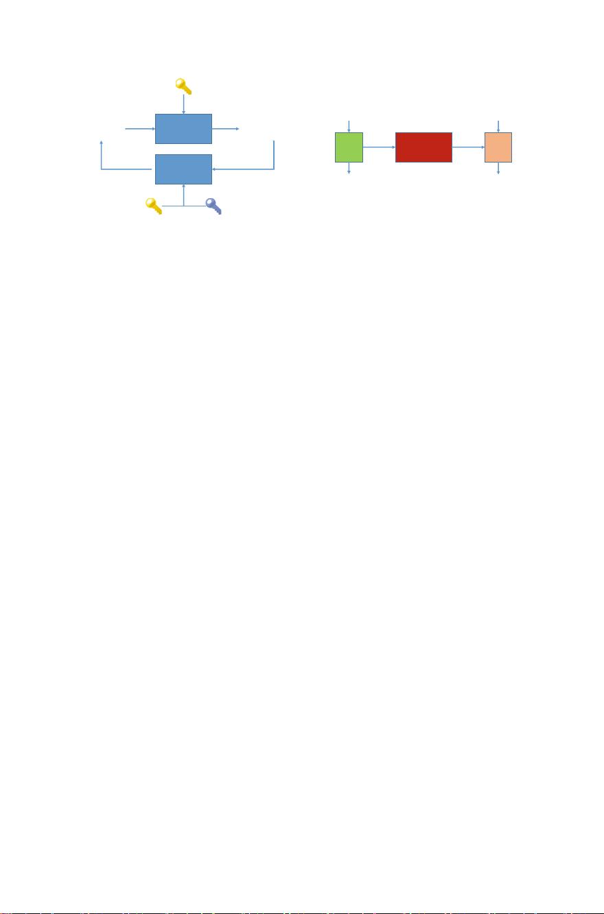
EncrypƟon
Plaintext
( Hello There! )
Ciphertext
( 4R$w#!#@$H65 )
DecrypƟon
Symmetric Asymmetric
(i)
Obfuscator
O
F F’
In
( How are you? )
Out
( Good! )
(ii)
In
( How are you? )
Out
( Good! )
Fig. 1.1 a Encryption. b Obfuscation
an attacker to use the obfuscated program O(P) as a virtual black box and is only
concerned with the protection of the program P. Obfuscators are also commonly
used in the context of obfuscating programs that implement an algorithm as opposed
to general data (e.g., user information/authentication and passwords) that encryption
can be used for.
Unfortunately, one major weakness that obfuscation has in relation to encryption
is that the security of obfuscation techniques cannot be reduced to mathematically
‘hard’ problems such as integer factorization for RSA. In a landmark paper [5], it was
shown that the general notion of virtual black-box obfuscation is not achievable for
all programs. The authors argued that there exists a family of functions (represented
as boolean circuits) that were inherently ‘unobfuscatable.’ In other words, given
a program P
that computes the s ame input–output relationship as P, the attacker
can feasibly reconstruct P or extract a secret s from P
about P with non-negligible
probability. This means that unlike encryption, which does not prevent any set of
data from being encrypted securely, obfuscation is not a universal operation.
1.1.1.3 Alternative Definitions
In spite of the above, later work has shown that although ‘all functions’ cannot be
securely obfuscated (reduced to a ‘hard’ computational problem), some functions
(such as a point function, which can be thought of as a password checking program)
can be securely obfuscated [6]. Later, the authors in [7] showed that the virtual
black-box property, which implies that the program should leak absolutely no other
information than its input–output relationship, might be too strong to be achievable
in practice. They proposed a relaxed definition termed as ‘best possible obfuscation’
which states that an obfuscated program O (P) implementing a function F can leak as
little information as any other program that computes the same function F. In other
words, an adversary can learn no more information about the obfuscated program
O(P) than he or she can learn from any other program computing the same function.


剩余351页未读,继续阅读

soctest2010
- 粉丝: 0
- 资源: 6
 我的内容管理
展开
我的内容管理
展开


最新资源
- 构建Cadence PSpice仿真模型库教程
- VMware 10.0安装指南:步骤详解与网络、文件共享解决方案
- 中国互联网20周年必读:影响行业的100本经典书籍
- SQL Server 2000 Analysis Services的经典MDX查询示例
- VC6.0 MFC操作Excel教程:亲测Win7下的应用与保存技巧
- 使用Python NetworkX处理网络图
- 科技驱动:计算机控制技术的革新与应用
- MF-1型机器人硬件与robobasic编程详解
- ADC性能指标解析:超越位数、SNR和谐波
- 通用示波器改造为逻辑分析仪:0-1字符显示与电路设计
- C++实现TCP控制台客户端
- SOA架构下ESB在卷烟厂的信息整合与决策支持
- 三维人脸识别:技术进展与应用解析
- 单张人脸图像的眼镜边框自动去除方法
- C语言绘制图形:余弦曲线与正弦函数示例
- Matlab 文件操作入门:fopen、fclose、fprintf、fscanf 等函数使用详解
资源上传下载、课程学习等过程中有任何疑问或建议,欢迎提出宝贵意见哦~我们会及时处理!
点击此处反馈


