AN430 Verilog
时间: 2023-11-08 13:23:09 浏览: 75
AN430 is a document published by Microchip Technology Inc. that provides a guide to implement a low-cost, low-power, and high-performance UART (Universal Asynchronous Receiver/Transmitter) module using Verilog hardware description language (HDL) on their PIC32 microcontrollers. The document includes a detailed explanation of the design, hardware and software requirements, simulation and verification, and final implementation of the UART module using Verilog. It also includes Verilog source code for the UART module. The AN430 document is intended for users who have basic knowledge of Verilog and HDL design.
相关问题
AN430 Verilog驱动
AN430是Microchip公司发布的一篇应用笔记,其中提供了使用Verilog语言编写驱动程序的示例。这篇应用笔记主要介绍了如何通过Verilog驱动来控制Microchip公司的SPI Flash器件。
Verilog是一种硬件描述语言,主要用于数字电路设计和FPGA/CPLD编程。使用Verilog编写驱动程序可以使硬件设计师更加方便地控制外部设备,例如该应用笔记中提到的SPI Flash器件。
该应用笔记中提供了完整的Verilog代码示例,包括模块声明、时序图和状态机图等。此外,还提供了详细的说明和注释,方便读者理解代码的实现细节和逻辑。
如果您需要使用Verilog编写驱动程序来控制外部设备,可以参考该应用笔记中的示例代码。同时,也可以参考其他相关的Verilog教程和资料,深入学习和掌握Verilog语言的使用方法。
verilog mar_a1 is an unknow type
在Verilog HDL(Hardware Description Language)中,"mar_a1 is an unknown type"是一个错误提示,通常表示编译器无法识别变量或模块名`mar_a1`所指的数据类型。这可能是由于以下几个原因:
1. 类型未定义:`mar_a1`可能期望是一个已定义的数据类型,如`reg`, `wire`, `integer`, `time`等,如果没有明确指定类型,就会报错。
2. 拼写或大小写错误:检查`mar_a1`的名称是否存在拼写错误,以及大小写的匹配性,因为Verilog是大小写敏感的。
3. 导入包含该类型的库或模块:如果你在一个模块内部引用了另一个模块中的类型,确保已经正确地导入了相应的库或包含了对应的模块。
4. 定义的位置问题:检查`mar_a1`的定义是否在其作用域内,例如,在模块内部定义了一个变量,但在外部尝试访问它。
修复这个问题的一般步骤是:
- 确认`mar_a1`的类型,并在需要的地方显式指定。
- 检查命名是否正确,避免拼写错误或大小写问题。
- 如果`mar_a1`是从其他模块导入的类型,确保正确的导入路径。
例子:
```verilog
module example (
input reg mar_a1, // 显示这是一个reg类型的输入
//...
);
// 或者
wire mar_a1 : some_custom_type; // 如果mar_a1是自定义的数据类型
//...
endmodule
```
阅读全文
相关推荐
最新推荐
JavaScript实现的高效pomodoro时钟教程
资源摘要信息:"JavaScript中的pomodoroo时钟"
知识点1:什么是番茄工作法
番茄工作法是一种时间管理技术,它是由弗朗西斯科·西里洛于1980年代末发明的。该技术使用一个定时器来将工作分解为25分钟的块,这些时间块之间短暂休息。每个时间块被称为一个“番茄”,因此得名“番茄工作法”。该技术旨在帮助人们通过短暂的休息来提高集中力和生产力。
知识点2:JavaScript是什么
JavaScript是一种高级的、解释执行的编程语言,它是网页开发中最主要的技术之一。JavaScript主要用于网页中的前端脚本编写,可以实现用户与浏览器内容的交云互动,也可以用于服务器端编程(Node.js)。JavaScript是一种轻量级的编程语言,被设计为易于学习,但功能强大。
知识点3:使用JavaScript实现番茄钟的原理
在使用JavaScript实现番茄钟的过程中,我们需要用到JavaScript的计时器功能。JavaScript提供了两种计时器方法,分别是setTimeout和setInterval。setTimeout用于在指定的时间后执行一次代码块,而setInterval则用于每隔一定的时间重复执行代码块。在实现番茄钟时,我们可以使用setInterval来模拟每25分钟的“番茄时间”,使用setTimeout来控制每25分钟后的休息时间。
知识点4:如何在JavaScript中设置和重置时间
在JavaScript中,我们可以使用Date对象来获取和设置时间。Date对象允许我们获取当前的日期和时间,也可以让我们创建自己的日期和时间。我们可以通过new Date()创建一个新的日期对象,并使用Date对象提供的各种方法,如getHours(), getMinutes(), setHours(), setMinutes()等,来获取和设置时间。在实现番茄钟的过程中,我们可以通过获取当前时间,然后加上25分钟,来设置下一个番茄时间。同样,我们也可以通过获取当前时间,然后减去25分钟,来重置上一个番茄时间。
知识点5:实现pomodoro-clock的基本步骤
首先,我们需要创建一个定时器,用于模拟25分钟的工作时间。然后,我们需要在25分钟结束后提醒用户停止工作,并开始短暂的休息。接着,我们需要为用户的休息时间设置另一个定时器。在用户休息结束后,我们需要重置定时器,开始下一个工作周期。在这个过程中,我们需要为每个定时器设置相应的回调函数,以处理定时器触发时需要执行的操作。
知识点6:使用JavaScript实现pomodoro-clock的优势
使用JavaScript实现pomodoro-clock的优势在于JavaScript的轻量级和易学性。JavaScript作为前端开发的主要语言,几乎所有的现代浏览器都支持JavaScript。因此,我们可以很容易地在网页中实现pomodoro-clock,用户只需要打开网页即可使用。此外,JavaScript的灵活性也使得我们可以根据需要自定义pomodoro-clock的各种参数,如工作时间长度、休息时间长度等。
管理建模和仿真的文件
管理Boualem Benatallah引用此版本:布阿利姆·贝纳塔拉。管理建模和仿真。约瑟夫-傅立叶大学-格勒诺布尔第一大学,1996年。法语。NNT:电话:00345357HAL ID:电话:00345357https://theses.hal.science/tel-003453572008年12月9日提交HAL是一个多学科的开放存取档案馆,用于存放和传播科学研究论文,无论它们是否被公开。论文可以来自法国或国外的教学和研究机构,也可以来自公共或私人研究中心。L’archive ouverte pluridisciplinaire
【WebLogic客户端兼容性提升秘籍】:一站式解决方案与实战案例
# 摘要
WebLogic作为一款广泛使用的中间件产品,其客户端兼容性对于企业应用至关重要。本文从基本概念出发,系统地介绍了WebLogic的架构、组件以及兼容性问题的分类和影响。通过深入分析兼容性测试方法和诊断分析技术,探讨了如何有效地识别和解决客户端兼容性问题。进一步,本文提出了提升兼容性的策略,包括代码层面的设计、配置管理、补丁升级以及快速响应流程。最后,结合实战案例,本文详细说明了解决方案的实施过
使用jupyter读取文件“近5年考试人数.csv”,绘制近5年高考及考研人数发展趋势图,数据如下(单位:万人)。
在Jupyter Notebook中读取CSV文件并绘制图表,通常需要几个步骤:
1. 首先,你需要导入必要的库,如pandas用于数据处理,matplotlib或seaborn用于数据可视化。
```python
import pandas as pd
import matplotlib.pyplot as plt
```
2. 使用`pd.read_csv()`函数加载CSV文件:
```python
df = pd.read_csv('近5年考试人数.csv')
```
3. 确保数据已经按照年份排序,如果需要的话,可以添加这一行:
```python
df = df.sor
CMake 3.25.3版本发布:程序员必备构建工具
资源摘要信息:"Cmake-3.25.3.zip文件是一个包含了CMake软件版本3.25.3的压缩包。CMake是一个跨平台的自动化构建系统,用于管理软件的构建过程,尤其是对于C++语言开发的项目。CMake使用CMakeLists.txt文件来配置项目的构建过程,然后可以生成不同操作系统的标准构建文件,如Makefile(Unix系列系统)、Visual Studio项目文件等。CMake广泛应用于开源和商业项目中,它有助于简化编译过程,并支持生成多种开发环境下的构建配置。
CMake 3.25.3版本作为该系列软件包中的一个点,是CMake的一个稳定版本,它为开发者提供了一系列新特性和改进。随着版本的更新,3.25.3版本可能引入了新的命令、改进了用户界面、优化了构建效率或解决了之前版本中发现的问题。
CMake的主要特点包括:
1. 跨平台性:CMake支持多种操作系统和编译器,包括但不限于Windows、Linux、Mac OS、FreeBSD、Unix等。
2. 编译器独立性:CMake生成的构建文件与具体的编译器无关,允许开发者在不同的开发环境中使用同一套构建脚本。
3. 高度可扩展性:CMake能够使用CMake模块和脚本来扩展功能,社区提供了大量的模块以支持不同的构建需求。
4. CMakeLists.txt:这是CMake的配置脚本文件,用于指定项目源文件、库依赖、自定义指令等信息。
5. 集成开发环境(IDE)支持:CMake可以生成适用于多种IDE的项目文件,例如Visual Studio、Eclipse、Xcode等。
6. 命令行工具:CMake提供了命令行工具,允许用户通过命令行对构建过程进行控制。
7. 可配置构建选项:CMake支持构建选项的配置,使得用户可以根据需要启用或禁用特定功能。
8. 包管理器支持:CMake可以从包管理器中获取依赖,并且可以使用FetchContent或ExternalProject模块来获取外部项目。
9. 测试和覆盖工具:CMake支持添加和运行测试,并集成代码覆盖工具,帮助开发者对代码进行质量控制。
10. 文档和帮助系统:CMake提供了一个内置的帮助系统,可以为用户提供命令和变量的详细文档。
CMake的安装和使用通常分为几个步骤:
- 下载并解压对应平台的CMake软件包。
- 在系统中配置CMake的环境变量,确保在命令行中可以全局访问cmake命令。
- 根据项目需要编写CMakeLists.txt文件。
- 在含有CMakeLists.txt文件的目录下执行cmake命令生成构建文件。
- 使用生成的构建文件进行项目的构建和编译工作。
CMake的更新和迭代通常会带来更好的用户体验和更高效的构建过程。对于开发者而言,及时更新到最新稳定版本的CMake是保持开发效率和项目兼容性的重要步骤。而对于新用户,掌握CMake的使用则是学习现代软件构建技术的一个重要方面。"
"互动学习:行动中的多样性与论文攻读经历"
多样性她- 事实上SCI NCES你的时间表ECOLEDO C Tora SC和NCESPOUR l’Ingén学习互动,互动学习以行动为中心的强化学习学会互动,互动学习,以行动为中心的强化学习计算机科学博士论文于2021年9月28日在Villeneuve d'Asq公开支持马修·瑟林评审团主席法布里斯·勒菲弗尔阿维尼翁大学教授论文指导奥利维尔·皮耶昆谷歌研究教授:智囊团论文联合主任菲利普·普雷教授,大学。里尔/CRISTAL/因里亚报告员奥利维耶·西格德索邦大学报告员卢多维奇·德诺耶教授,Facebook /索邦大学审查员越南圣迈IMT Atlantic高级讲师邀请弗洛里安·斯特鲁布博士,Deepmind对于那些及时看到自己错误的人...3谢谢你首先,我要感谢我的两位博士生导师Olivier和Philippe。奥利维尔,"站在巨人的肩膀上"这句话对你来说完全有意义了。从科学上讲,你知道在这篇论文的(许多)错误中,你是我可以依
数字信号处理全攻略:掌握15个关键技巧,提升你的处理效率
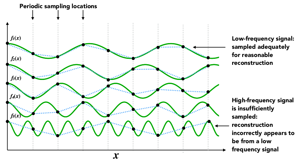
# 摘要
数字信号处理作为信息科技领域的重要分支,涵盖了从基础理论到高级应用的广泛内容。本文首先介绍了数字信号处理的基础知识,包括基本概念、时域与频域分析、以及核心算法和理论框架。接着,详细探讨了实现信号采样和量化、滤波器设计、以及信号增强和重建实践技巧。文章进一步深入到高级应用,包括信号压缩技术、多维信号处理,以及人工智能技术在信号处理中的集成。最后,本文评述了数字信号处理
给定不超过6的正整数A,考虑从A开始的连续4个数字。请输出所有由它们组成的无重复数字的3位数。编写一个C语言程序
为了编写一个C语言程序来解决这个问题,我们需要遍历给定范围内的所有连续4个数字,并检查每个组合是否能构成一个无重复数字的三位数。这里是一个简单的示例程序:
```c
#include <stdio.h>
// 函数定义,用于生成并检查无重复数字的3位数
void generate_unique_3_digit(int A) {
for (int i = A; i <= A + 3; i++) {
int num = i * 100 + (i+1) * 10 + (i+2);
if (num >= 100 && num < 1000 && is_uni
直流无刷电机控制技术项目源码集合
资源摘要信息:"直流无刷实例源码.zip"
该资源为一个包含多个技术项目源码的压缩文件,涵盖了IT技术的多个领域。接下来将详细介绍这些领域,并对其在源码中的应用进行说明。
1. 前端开发:前端开发通常指使用HTML、CSS和JavaScript等技术进行网页界面的构建。前端源码可能包括实现用户交互界面的代码,响应式布局实现,以及一些前端框架(如React或Vue.js)的使用实例。
2. 后端开发:后端通常涉及服务器端的编程,使用如PHP、Java、Python、C#等语言,处理HTTP请求、数据库交互、业务逻辑实现等。源码中可能包含服务器的搭建、数据库设计、API接口的实现等方面的内容。
3. 移动开发:移动开发关注于移动设备上的应用开发,涉及iOS、Android等平台,使用Swift、Kotlin、Java或跨平台框架如Flutter等。源码可能包括移动界面的布局、触摸事件处理、应用与后端数据的交互等。
4. 操作系统:操作系统源码可能包括对Linux内核的修改、或是基于RTOS(实时操作系统)的嵌入式系统开发。这类源码往往更偏向底层,涉及系统级编程。
5. 人工智能:人工智能项目源码可能包含机器学习、深度学习的实现,使用Python的TensorFlow或PyTorch框架等。这些源码可能涉及图像识别、自然语言处理等复杂算法的实现。
6. 物联网:物联网项目源码可能包含设备端与云平台的数据交互,使用的技术可能包括MQTT协议、HTTP/HTTPS协议等,可能还会涉及ESP8266这样的Wi-Fi模块使用。
7. 信息化管理:这类项目源码可能包含企业信息系统的构建,使用的技术可能包括数据库操作、数据报表生成、工作流管理等。
8. 数据库:数据库源码可能包括数据库的设计、操作,比如使用MySQL、PostgreSQL、MongoDB等数据库系统的SQL编写、存储过程、触发器等。
9. 硬件开发:硬件开发源码可能涉及使用STM32微控制器、EDA工具(如Proteus)进行电路设计、模拟和编程。
10. 大数据:大数据源码可能包含数据采集、存储、处理和分析的过程,可能会用到Hadoop、Spark、Flink等大数据处理框架。
11. 课程资源:这部分源码可能是为教学目的设计的,它可能包括一些基本项目的实现,适合初学者学习和理解。
12. 音视频:音视频源码可能包括音视频播放、录制、编解码等技术的应用,可能涉及到webRTC、FFmpeg等技术。
13. 网站开发:网站开发源码可能包括从简单的静态页面到复杂的动态网站实现,涉及前端框架、后端逻辑、数据库交互等。
14. EDA:电子设计自动化(EDA)源码可能包括电路图设计、PCB布线等,使用如Altium Designer、Eagle等专业EDA工具。
15. Proteus:Proteus源码可能包括电路的模拟和测试,它可以模拟微控制器和其他电子元件的行为。
该资源所包含的项目源码均已通过严格测试,可以直接运行。源码的适用人群广泛,不仅适合初学者学习不同技术领域,也适合进阶学习者或专业人士作为参考或直接拿来修改扩展,实现新功能。所有源码的上传都经过确认其正常工作,确保下载者可以直接使用。
在使用这些源码时,如果遇到任何问题,可以随时与博主沟通,博主将提供及时的解答。此外,鼓励用户下载和使用这些资源,互相学习、共同进步。
由于压缩文件的文件名称列表中只提供了"直流无刷实例源码",没有具体项目名称,因此我们无法得知具体的项目实例。然而,根据文件描述,我们可以确定这些源码项目覆盖了从硬件到软件、从传统应用到现代技术的广泛范围,并且针对了直流无刷电机的控制实例进行了特别的说明。
请注意,由于资源的宽泛涵盖性,这里提供的信息并不包含特定项目的详细分析,而是根据描述中的关键词进行了技术领域的概括性描述。如果需要针对具体项目进行分析,建议下载资源并根据具体文件内容进行详细探讨。
关系数据表示学习
关系数据卢多维奇·多斯桑托斯引用此版本:卢多维奇·多斯桑托斯。关系数据的表示学习机器学习[cs.LG]。皮埃尔和玛丽·居里大学-巴黎第六大学,2017年。英语。NNT:2017PA066480。电话:01803188HAL ID:电话:01803188https://theses.hal.science/tel-01803188提交日期:2018年HAL是一个多学科的开放存取档案馆,用于存放和传播科学研究论文,无论它们是否被公开。论文可以来自法国或国外的教学和研究机构,也可以来自公共或私人研究中心。L’archive ouverte pluridisciplinaireUNIVERSITY PIERRE和 MARIE CURIE计算机科学、电信和电子学博士学院(巴黎)巴黎6号计算机科学实验室D八角形T HESIS关系数据表示学习作者:Ludovic DOS SAntos主管:Patrick GALLINARI联合主管:本杰明·P·伊沃瓦斯基为满足计算机科学博士学位的要求而提交的论文评审团成员:先生蒂埃里·A·退休记者先生尤尼斯·B·恩