PE_DAT bit 31:13 12:0 R/W R/W Default/Hex 0 reserved if the port is configured as inrit,the corresponding bit is the pin state.if the port is configured as output, the pin state is the same as the corresponding bit. the read bit value is the vlaue setu by software.if the port is configured as functional pin,the undefined value will be read.这个寄存器如何用
时间: 2024-03-28 20:40:17 浏览: 52
这是一个关于 GPIO(通用输入/输出)端口的寄存器描述。该寄存器的位字段描述了 GPIO 端口的输入/输出状态。其中,bit 31:13 是保留位,不可用。bit 12:0 是可读/可写位,对应 GPIO 端口的状态。
如果 GPIO 端口被配置为输入模式,那么对应的位就是对应引脚的状态。如果 GPIO 端口被配置为输出模式,那么对应的位的值就是输出到对应引脚的状态。当读取该位时,返回的值是由软件设置的值。如果 GPIO 端口被配置为功能引脚,那么这个位的值是未定义的。
因此,使用这个寄存器可以控制 GPIO 端口的输入/输出状态,使其可以实现各种功能,如控制 LED 灯的亮灭、读取开关状态等等。需要根据具体的硬件平台和应用场景,结合具体的 GPIO 端口的定义,使用该寄存器进行配置和控制。
相关问题
参数有 offset 0x90 PE2 BIT 11 10:8 R/W R/W default/Hex 7 Res erved 001out 如何设置PE2为输出模式
要将PE2设置为输出模式,需要将BIT 11:9设置为输出方向控制位。具体来说,需要将这三位设置为0b001,表示将PE2设置为输出方向。可以使用如下代码实现:
```
// 将BIT 11:9设置为0b001
GPIOE->MODER &= ~(3 << (2 * 2)); // 清零原来的值
GPIOE->MODER |= (1 << (2 * 2)); // 设置为输出模式
// 将PE2设置为默认输出值
GPIOE->ODR &= ~(1 << 2); // 清零PE2
GPIOE->ODR |= (1 << 2); // 设置PE2为默认输出值(1)
```
其中,`GPIOE`表示GPIOE的寄存器地址,`MODER`表示GPIOE的模式寄存器,`ODR`表示GPIOE的输出寄存器。`2 * 2`表示PE2在寄存器中的偏移量,`1 << (2 * 2)`表示将对应位设置为1,`~(1 << 2)`表示将对应位设置为0。
module seg( input wire clk , //100MHz input wire rst_n , //low valid input wire [17:0] data_in , //待显示数据 output reg [6:0] hex1 , // -共阳极,低电平有效 output reg [6:0] hex2 , // - output reg [6:0] hex3 , // - output reg [6:0] hex4 //熄灭 ); //parameter define localparam NUM_0 = 8'b1100_0000, NUM_1 = 8'b1111_1001, NUM_2 = 8'b1010_0100, NUM_3 = 8'b1011_0000, NUM_4 = 8'b1001_1001, NUM_5 = 8'b1001_0010, NUM_6 = 8'b1000_0010, NUM_7 = 8'b1111_1000, NUM_8 = 8'b1000_0000, NUM_9 = 8'b1001_0000, NUM_A = 8'b1000_1000, NUM_B = 8'b1000_0011, NUM_C = 8'b1100_0110, NUM_D = 8'b1010_0001, NUM_E = 8'b1000_0110, NUM_F = 8'b1000_1110, ALL_LIGHT = 8'b0000_0000, LIT_OUT = 8'b1111_1111; //reg 、wire define reg [3:0] cm_hund ;//100cm reg [3:0] cm_ten ;//10cm reg [3:0] cm_unit ;//1cm always @(posedge clk or negedge rst_n)begin if(!rst_n)begin cm_hund <= 'd0; cm_ten <= 'd0; cm_unit <= 'd0; end else begin cm_hund <= data_in / 10 ** 2; cm_ten <= data_in / 10**1 % 10; cm_unit <= data_in/10**0 % 10; end end always @(posedge clk or negedge rst_n)begin if(!rst_n)begin hex1 <= ALL_LIGHT; hex2 <= ALL_LIGHT; hex3 <= ALL_LIGHT; hex4 <= ALL_LIGHT; end else begin hex1 <= hex_data(cm_unit); hex2 <= hex_data(cm_ten); hex3 <= hex_data(cm_hund); hex4 <= LIT_OUT; end end //always end function [6:0] hex_data; //函数不含时序逻辑相关 input [03:00] data_i;//至少一个输入 begin case(data_i) 'd0:hex_data = NUM_0; 'd1:hex_data = NUM_1; 'd2:hex_data = NUM_2; 'd3:hex_data = NUM_3; 'd4:hex_data = NUM_4; 'd5:hex_data = NUM_5; 'd6:hex_data = NUM_6; 'd7:hex_data = NUM_7; 'd8:hex_data = NUM_8; 'd9:hex_data = NUM_9; default:hex_data = ALL_LIGHT; endcase end endfunction endmodule
这是一个Verilog HDL写的模块,可以实现数字显示器的功能。其中,模块的输入包括时钟信号clk、复位信号rst_n和待显示的数据data_in,输出包括4个七段数码管的控制信号hex1、hex2、hex3和hex4。模块中使用了parameter定义常量和reg、wire定义寄存器和线网,同时使用了always块和function函数实现时序逻辑和数字转换功能。具体实现是将待显示的数据转换为3个数字,然后通过函数将数字转换为对应的七段数码管控制信号。
阅读全文
相关推荐
最新推荐
A级景区数据文件json
A级景区数据文件json
使用Java编写的坦克大战小游戏.zip学习资料
python
使用Java编写的坦克大战小游戏.zip学习资料
【python毕设】p073基于Spark的温布尔登特色赛赛事数据分析预测及算法实现_flask(5).zip
项目资源包含:可运行源码+sql文件+; python3.7+flask+spark+mysql5.7+vue
适用人群:学习不同技术领域的小白或进阶学习者;可作为毕设项目、课程设计、大作业、工程实训或初期项目立项。
项目具有较高的学习借鉴价值,也可拿来修改、二次开发。
有任何使用上的问题,欢迎随时与博主沟通,博主看到后会第一时间及时解答。
系统是一个很好的项目,结合了后端服务(flask)和前端用户界面(Vue.js)技术,实现了前后端分离。
后台路径地址:localhost:8080/项目名称/admin/dist/index.html
前台路径地址:localhost:8080/项目名称/front/index.html
JHU荣誉单变量微积分课程教案介绍
资源摘要信息:"jhu2017-18-honors-single-variable-calculus"
知识点一:荣誉单变量微积分课程介绍
本课程为JHU(约翰霍普金斯大学)的荣誉单变量微积分课程,主要针对在2018年秋季和2019年秋季两个学期开设。课程内容涵盖两个学期的微积分知识,包括整合和微分两大部分。该课程采用IBL(Inquiry-Based Learning)格式进行教学,即学生先自行解决问题,然后在学习过程中逐步掌握相关理论知识。
知识点二:IBL教学法
IBL教学法,即问题导向的学习方法,是一种以学生为中心的教学模式。在这种模式下,学生在教师的引导下,通过提出问题、解决问题来获取知识,从而培养学生的自主学习能力和问题解决能力。IBL教学法强调学生的主动参与和探索,教师的角色更多的是引导者和协助者。
知识点三:课程难度及学习方法
课程的第一次迭代主要包含问题,难度较大,学生需要有一定的数学基础和自学能力。第二次迭代则在第一次的基础上增加了更多的理论和解释,难度相对降低,更适合学生理解和学习。这种设计旨在帮助学生从实际问题出发,逐步深入理解微积分理论,提高学习效率。
知识点四:课程先决条件及学习建议
课程的先决条件为预演算,即在进入课程之前需要掌握一定的演算知识和技能。建议在使用这些笔记之前,先完成一些基础演算的入门课程,并进行一些数学证明的练习。这样可以更好地理解和掌握课程内容,提高学习效果。
知识点五:TeX格式文件
标签"TeX"意味着该课程的资料是以TeX格式保存和发布的。TeX是一种基于排版语言的格式,广泛应用于学术出版物的排版,特别是在数学、物理学和计算机科学领域。TeX格式的文件可以确保文档内容的准确性和排版的美观性,适合用于编写和分享复杂的科学和技术文档。
管理建模和仿真的文件
管理Boualem Benatallah引用此版本:布阿利姆·贝纳塔拉。管理建模和仿真。约瑟夫-傅立叶大学-格勒诺布尔第一大学,1996年。法语。NNT:电话:00345357HAL ID:电话:00345357https://theses.hal.science/tel-003453572008年12月9日提交HAL是一个多学科的开放存取档案馆,用于存放和传播科学研究论文,无论它们是否被公开。论文可以来自法国或国外的教学和研究机构,也可以来自公共或私人研究中心。L’archive ouverte pluridisciplinaire
【实战篇:自定义损失函数】:构建独特损失函数解决特定问题,优化模型性能
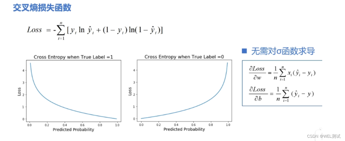
# 1. 损失函数的基本概念与作用
## 1.1 损失函数定义
损失函数是机器学习中的核心概念,用于衡量模型预测值与实际值之间的差异。它是优化算法调整模型参数以最小化的目标函数。
```math
L(y, f(x)) = \sum_{i=1}^{N} L_i(y_i, f(x_i))
```
其中,`L`表示损失函数,`y`为实际值,`f(x)`为模型预测值,`N`为样本数量,`L_i`为第`i`个样本的损失。
## 1.2 损
如何在ZYNQMP平台上配置TUSB1210 USB接口芯片以实现Host模式,并确保与Linux内核的兼容性?
要在ZYNQMP平台上实现TUSB1210 USB接口芯片的Host模式功能,并确保与Linux内核的兼容性,首先需要在硬件层面完成TUSB1210与ZYNQMP芯片的正确连接,保证USB2.0和USB3.0之间的硬件电路设计符合ZYNQMP的要求。
参考资源链接:[ZYNQMP USB主机模式实现与测试(TUSB1210)](https://wenku.csdn.net/doc/6nneek7zxw?spm=1055.2569.3001.10343)
具体步骤包括:
1. 在Vivado中设计硬件电路,配置USB接口相关的Bank502和Bank505引脚,同时确保USB时钟的正确配置。
Naruto爱好者必备CLI测试应用
资源摘要信息:"Are-you-a-Naruto-Fan:CLI测验应用程序,用于检查Naruto狂热者的知识"
该应用程序是一个基于命令行界面(CLI)的测验工具,设计用于测试用户对日本动漫《火影忍者》(Naruto)的知识水平。《火影忍者》是由岸本齐史创作的一部广受欢迎的漫画系列,后被改编成同名电视动画,并衍生出一系列相关的产品和文化现象。该动漫讲述了主角漩涡鸣人从忍者学校开始的成长故事,直到成为木叶隐村的领袖,期间包含了忍者文化、战斗、忍术、友情和忍者世界的政治斗争等元素。
这个测验应用程序的开发主要使用了JavaScript语言。JavaScript是一种广泛应用于前端开发的编程语言,它允许网页具有交互性,同时也可以在服务器端运行(如Node.js环境)。在这个CLI应用程序中,JavaScript被用来处理用户的输入,生成问题,并根据用户的回答来评估其对《火影忍者》的知识水平。
开发这样的测验应用程序可能涉及到以下知识点和技术:
1. **命令行界面(CLI)开发:** CLI应用程序是指用户通过命令行或终端与之交互的软件。在Web开发中,Node.js提供了一个运行JavaScript的环境,使得开发者可以使用JavaScript语言来创建服务器端应用程序和工具,包括CLI应用程序。CLI应用程序通常涉及到使用诸如 commander.js 或 yargs 等库来解析命令行参数和选项。
2. **JavaScript基础:** 开发CLI应用程序需要对JavaScript语言有扎实的理解,包括数据类型、函数、对象、数组、事件循环、异步编程等。
3. **知识库构建:** 测验应用程序的核心是其问题库,它包含了与《火影忍者》相关的各种问题。开发人员需要设计和构建这个知识库,并确保问题的多样性和覆盖面。
4. **逻辑和流程控制:** 在应用程序中,需要编写逻辑来控制测验的流程,比如问题的随机出现、计时器、计分机制以及结束时的反馈。
5. **用户界面(UI)交互:** 尽管是CLI,用户界面仍然重要。开发者需要确保用户体验流畅,这包括清晰的问题呈现、简洁的指令和友好的输出格式。
6. **模块化和封装:** 开发过程中应当遵循模块化原则,将不同的功能分隔开来,以便于管理和维护。例如,可以将问题生成器、计分器和用户输入处理器等封装成独立的模块。
7. **单元测试和调试:** 测验应用程序在发布前需要经过严格的测试和调试。使用如Mocha或Jest这样的JavaScript测试框架可以编写单元测试,并通过控制台输出调试信息来排除故障。
8. **部署和分发:** 最后,开发完成的应用程序需要被打包和分发。如果是基于Node.js的应用程序,常见的做法是将其打包为可执行文件(如使用electron或pkg工具),以便在不同的操作系统上运行。
根据提供的文件信息,虽然具体细节有限,但可以推测该应用程序可能采用了上述技术点。用户通过点击提供的链接,可能将被引导到一个网页或直接下载CLI应用程序的可执行文件,从而开始进行《火影忍者》的知识测验。通过这个测验,用户不仅能享受答题的乐趣,还可以加深对《火影忍者》的理解和认识。
"互动学习:行动中的多样性与论文攻读经历"
多样性她- 事实上SCI NCES你的时间表ECOLEDO C Tora SC和NCESPOUR l’Ingén学习互动,互动学习以行动为中心的强化学习学会互动,互动学习,以行动为中心的强化学习计算机科学博士论文于2021年9月28日在Villeneuve d'Asq公开支持马修·瑟林评审团主席法布里斯·勒菲弗尔阿维尼翁大学教授论文指导奥利维尔·皮耶昆谷歌研究教授:智囊团论文联合主任菲利普·普雷教授,大学。里尔/CRISTAL/因里亚报告员奥利维耶·西格德索邦大学报告员卢多维奇·德诺耶教授,Facebook /索邦大学审查员越南圣迈IMT Atlantic高级讲师邀请弗洛里安·斯特鲁布博士,Deepmind对于那些及时看到自己错误的人...3谢谢你首先,我要感谢我的两位博士生导师Olivier和Philippe。奥利维尔,"站在巨人的肩膀上"这句话对你来说完全有意义了。从科学上讲,你知道在这篇论文的(许多)错误中,你是我可以依
【强化学习损失函数探索】:奖励函数与损失函数的深入联系及优化策略
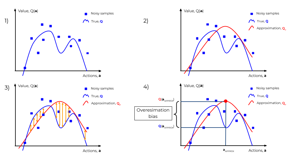
# 1. 强化学习中的损失函数基础
强化学习(Reinforcement Learning, RL)是机器学习领域的一个重要分支,它通过与环境的互动来学习如何在特定任务中做出决策。在强化学习中,损失函数(loss function)起着至关重要的作用,它是学习算法优化的关键所在。损失函数能够衡量智能体(agent)的策略(policy)表现,帮助智能体通过减少损失来改进自