verilog hdl设计半加器
时间: 2023-11-16 19:05:26 浏览: 204
--Outline--
I. Introduction
A. Description of a reader engrossed in a book
B. Debate on physical books vs. e-books vs. audiobooks
C. Question: Does the device affect the reader's reaction to the book?
II. Benefits of Reading
A. Areas of the brain used in reading
B. Strengthening of communicative ability, vocabulary, emotional intelligence, and social perception
III. Pros of Physical Books and E-books
A. Better retention of information
B. Ability to go back and find missed parts
IV. Pros of
相关问题
verilog两位半加器代码设计
在Verilog HDL中,设计一个两位半精度加法器(Half Adder Plus Borrow Register, HPBR)通常涉及以下几个步骤:
1. 定义模块(module):首先,我们需要定义一个名为`halfAdder`或类似名称的模块,它接受两个8位二进制数的输入A和B,并返回它们相加的结果Sum和进位 Carry。
```verilog
module half_adder(
input [7:0] A, // 8位输入A
input [7:0] B, // 8位输入B
output reg [7:0] Sum, // 累加结果
output reg C // 进位输出
);
```
2. 内部逻辑:接着,我们编写函数体,实现加法操作。对于半加器,我们只需要计算两个4位(高位两个)数字的和以及是否产生进位。这个可以通过与、异或门实现:
```verilog
wire [1:0] temp_sum; //临时结果
wire carry_in, carry_out;
temp_sum = A[6:5] ^ B[6:5]; // 高四位的按位异或
carry_in = A[4:3] & B[4:3]; // 高四位的低位是否进位
Sum[6:3] = temp_sum; // 存储高四位的结果
Sum[2:0] = A[2:0] ^ B[2:0]; // 低四位的按位异或
Sum[7] = carry_in; // 将进位信号存储到最高位
C = temp_sum[0]; // 最终的进位取决于上面临时结果的第一个比特
endmodule
```
3. 注释和端口连接:为了便于理解和维护,别忘了添加适当的注释,然后在模块外部将输入和输出端口连接到实际需要的地方。
```verilog
// ... 其他代码 ...
// 实例化half_adder模块
half_adder adder (
.A(A), // 连接输入A
.B(B), // 连接输入B
.Sum(Sum), // 连接累加结果Sum
.C(C) // 连接进位Carry
);
```
case语句实现一位半加器用Verilog HDL
module half_adder(A, B, SUM, CARRY);
input A, B;
output SUM, CARRY;
// case statement to implement half adder logic
case({A,B})
2'b00: begin
SUM = 1'b0;
CARRY = 1'b0;
end
2'b01: begin
SUM = 1'b1;
CARRY = 1'b0;
end
2'b10: begin
SUM = 1'b1;
CARRY = 1'b0;
end
2'b11: begin
SUM = 1'b0;
CARRY = 1'b1;
end
endcase
endmodule
阅读全文
相关推荐
最新推荐
【路径规划】狮群算法栅格地图机器人最短路径规划【含Matlab仿真 2863期】.zip
CSDN Matlab武动乾坤上传的资料均有对应的仿真结果图,仿真结果图均是完整代码运行得出,完整代码亲测可用,适合小白;
1、完整的代码压缩包内容
主函数:main.m;
调用函数:其他m文件;无需运行
运行结果效果图;
2、代码运行版本
Matlab 2019b;若运行有误,根据提示修改;若不会,私信博主;
3、运行操作步骤
步骤一:将所有文件放到Matlab的当前文件夹中;
步骤二:双击打开main.m文件;
步骤三:点击运行,等程序运行完得到结果;
4、仿真咨询
如需其他服务,可私信博主或扫描博客文章底部QQ名片;
4.1 博客或资源的完整代码提供
4.2 期刊或参考文献复现
4.3 Matlab程序定制
4.4 科研合作
MATLAB新功能:Multi-frame ViewRGB制作彩色图阴影
资源摘要信息:"MULTI_FRAME_VIEWRGB 函数是用于MATLAB开发环境下创建多帧彩色图像阴影的一个实用工具。该函数是MULTI_FRAME_VIEW函数的扩展版本,主要用于处理彩色和灰度图像,并且能够为多种帧创建图形阴影效果。它适用于生成2D图像数据的体视效果,以便于对数据进行更加直观的分析和展示。MULTI_FRAME_VIEWRGB 能够处理的灰度图像会被下采样为8位整数,以确保在处理过程中的高效性。考虑到灰度图像处理的特异性,对于灰度图像建议直接使用MULTI_FRAME_VIEW函数。MULTI_FRAME_VIEWRGB 函数的参数包括文件名、白色边框大小、黑色边框大小以及边框数等,这些参数可以根据用户的需求进行调整,以获得最佳的视觉效果。"
知识点详细说明:
1. MATLAB开发环境:MULTI_FRAME_VIEWRGB 函数是为MATLAB编写的,MATLAB是一种高性能的数值计算环境和第四代编程语言,广泛用于算法开发、数据可视化、数据分析以及数值计算等场合。在进行复杂的图像处理时,MATLAB提供了丰富的库函数和工具箱,能够帮助开发者高效地实现各种图像处理任务。
2. 图形阴影(Shadowing):在图像处理和计算机图形学中,阴影的添加可以使图像或图形更加具有立体感和真实感。特别是在多帧视图中,阴影的使用能够让用户更清晰地区分不同的数据层,帮助理解图像数据中的层次结构。
3. 多帧(Multi-frame):多帧图像处理是指对一系列连续的图像帧进行处理,以实现动态视觉效果或分析图像序列中的动态变化。在诸如视频、连续医学成像或动态模拟等场景中,多帧处理尤为重要。
4. RGB 图像处理:RGB代表红绿蓝三种颜色的光,RGB图像是一种常用的颜色模型,用于显示颜色信息。RGB图像由三个颜色通道组成,每个通道包含不同颜色强度的信息。在MULTI_FRAME_VIEWRGB函数中,可以处理彩色图像,并生成彩色图阴影,增强图像的视觉效果。
5. 参数调整:在MULTI_FRAME_VIEWRGB函数中,用户可以根据需要对参数进行调整,比如白色边框大小(we)、黑色边框大小(be)和边框数(ne)。这些参数影响着生成的图形阴影的外观,允许用户根据具体的应用场景和视觉需求,调整阴影的样式和强度。
6. 下采样(Downsampling):在处理图像时,有时会进行下采样操作,以减少图像的分辨率和数据量。在MULTI_FRAME_VIEWRGB函数中,灰度图像被下采样为8位整数,这主要是为了减少处理的复杂性和加快处理速度,同时保留图像的关键信息。
7. 文件名结构数组:MULTI_FRAME_VIEWRGB 函数使用文件名的结构数组作为输入参数之一。这要求用户提前准备好包含所有图像文件路径的结构数组,以便函数能够逐个处理每个图像文件。
8. MATLAB函数使用:MULTI_FRAME_VIEWRGB函数的使用要求用户具备MATLAB编程基础,能够理解函数的参数和输入输出格式,并能够根据函数提供的用法说明进行实际调用。
9. 压缩包文件名列表:在提供的资源信息中,有两个压缩包文件名称列表,分别是"multi_frame_viewRGB.zip"和"multi_fram_viewRGB.zip"。这里可能存在一个打字错误:"multi_fram_viewRGB.zip" 应该是 "multi_frame_viewRGB.zip"。需要正确提取压缩包中的文件,并且解压缩后正确使用文件名结构数组来调用MULTI_FRAME_VIEWRGB函数。
管理建模和仿真的文件
管理Boualem Benatallah引用此版本:布阿利姆·贝纳塔拉。管理建模和仿真。约瑟夫-傅立叶大学-格勒诺布尔第一大学,1996年。法语。NNT:电话:00345357HAL ID:电话:00345357https://theses.hal.science/tel-003453572008年12月9日提交HAL是一个多学科的开放存取档案馆,用于存放和传播科学研究论文,无论它们是否被公开。论文可以来自法国或国外的教学和研究机构,也可以来自公共或私人研究中心。L’archive ouverte pluridisciplinaire
【实战篇:自定义损失函数】:构建独特损失函数解决特定问题,优化模型性能
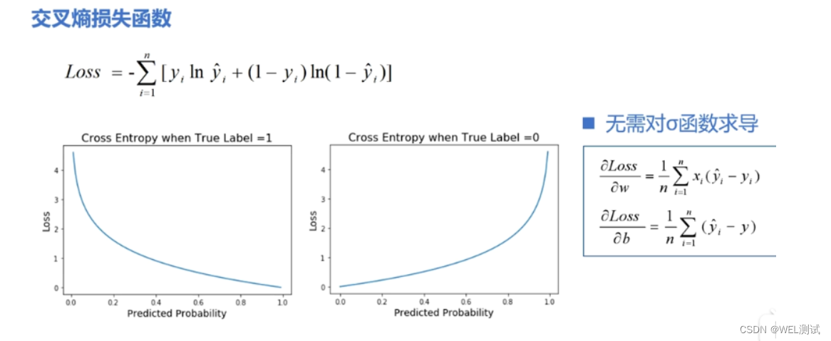
# 1. 损失函数的基本概念与作用
## 1.1 损失函数定义
损失函数是机器学习中的核心概念,用于衡量模型预测值与实际值之间的差异。它是优化算法调整模型参数以最小化的目标函数。
```math
L(y, f(x)) = \sum_{i=1}^{N} L_i(y_i, f(x_i))
```
其中,`L`表示损失函数,`y`为实际值,`f(x)`为模型预测值,`N`为样本数量,`L_i`为第`i`个样本的损失。
## 1.2 损
在Flow-3D中如何根据水利工程的特定需求设定边界条件和进行网格划分,以便准确模拟水流问题?
要在Flow-3D中设定合适的边界条件和进行精确的网格划分,首先需要深入理解水利工程的具体需求和流体动力学的基本原理。推荐参考《Flow-3D水利教程:边界条件设定与网格划分》,这份资料详细介绍了如何设置工作目录,创建模拟文档,以及进行网格划分和边界条件设定的全过程。
参考资源链接:[Flow-3D水利教程:边界条件设定与网格划分](https://wenku.csdn.net/doc/23xiiycuq6?spm=1055.2569.3001.10343)
在设置边界条件时,需要根据实际的水利工程项目来确定,如在模拟渠道流动时,可能需要设定速度边界条件或水位边界条件。对于复杂的
XKCD Substitutions 3-crx插件:创新的网页文字替换工具
资源摘要信息: "XKCD Substitutions 3-crx插件是一个浏览器扩展程序,它允许用户使用XKCD漫画中的内容替换特定网站上的单词和短语。XKCD是美国漫画家兰德尔·门罗创作的一个网络漫画系列,内容通常涉及幽默、科学、数学、语言和流行文化。XKCD Substitutions 3插件的核心功能是提供一个替换字典,基于XKCD漫画中的特定作品(如漫画1288、1625和1679)来替换文本,使访问网站的体验变得风趣并且具有教育意义。用户可以在插件的选项页面上自定义替换列表,以满足个人的喜好和需求。此外,该插件提供了不同的文本替换样式,包括无提示替换、带下划线的替换以及高亮显示替换,旨在通过不同的视觉效果吸引用户对变更内容的注意。用户还可以将特定网站列入黑名单,防止插件在这些网站上运行,从而避免在不希望干扰的网站上出现替换文本。"
知识点:
1. 浏览器扩展程序简介:
浏览器扩展程序是一种附加软件,可以增强或改变浏览器的功能。用户安装扩展程序后,可以在浏览器中添加新的工具或功能,比如自动填充表单、阻止弹窗广告、管理密码等。XKCD Substitutions 3-crx插件即为一种扩展程序,它专门用于替换网页文本内容。
2. XKCD漫画背景:
XKCD是由美国计算机科学家兰德尔·门罗创建的网络漫画系列。门罗以其独特的幽默感著称,漫画内容经常涉及科学、数学、工程学、语言学和流行文化等领域。漫画风格简洁,通常包含幽默和讽刺的元素,吸引了全球大量科技和学术界人士的关注。
3. 插件功能实现:
XKCD Substitutions 3-crx插件通过内置的替换规则集来实现文本替换功能。它通过匹配用户访问的网页中的单词和短语,并将其替换为XKCD漫画中的相应条目。例如,如果漫画1288、1625和1679中包含特定的短语或词汇,这些内容就可以被自动替换为插件所识别并替换的文本。
4. 用户自定义替换列表:
插件允许用户访问选项页面来自定义替换列表,这意味着用户可以根据自己的喜好添加、删除或修改替换规则。这种灵活性使得XKCD Substitutions 3成为一个高度个性化的工具,用户可以根据个人兴趣和阅读习惯来调整插件的行为。
5. 替换样式与用户体验:
插件提供了多种文本替换样式,包括无提示替换、带下划线的替换以及高亮显示替换。每种样式都有其特定的用户体验设计。无提示替换适用于不想分散注意力的用户;带下划线的替换和高亮显示替换则更直观地突出显示了被替换的文本,让更改更为明显,适合那些希望追踪替换效果的用户。
6. 黑名单功能:
为了避免在某些网站上无意中干扰网页的原始内容,XKCD Substitutions 3-crx插件提供了黑名单功能。用户可以将特定的域名加入黑名单,防止插件在这些网站上运行替换功能。这样可以保证用户在需要专注阅读的网站上,如工作相关的平台或个人兴趣网站,不会受到插件内容替换的影响。
7. 扩展程序与网络安全:
浏览器扩展程序可能会涉及到用户数据和隐私安全的问题。因此,安装和使用任何第三方扩展程序时,用户都应该确保来源的安全可靠,避免授予不必要的权限。同时,了解扩展程序的权限范围和它如何处理用户数据对于保护个人隐私是至关重要的。
通过这些知识点,可以看出XKCD Substitutions 3-crx插件不仅仅是一个简单的文本替换工具,而是一个结合了个人化定制、交互体验设计以及用户隐私保护的实用型扩展程序。它通过幽默风趣的XKCD漫画内容为用户带来不一样的网络浏览体验。
"互动学习:行动中的多样性与论文攻读经历"
多样性她- 事实上SCI NCES你的时间表ECOLEDO C Tora SC和NCESPOUR l’Ingén学习互动,互动学习以行动为中心的强化学习学会互动,互动学习,以行动为中心的强化学习计算机科学博士论文于2021年9月28日在Villeneuve d'Asq公开支持马修·瑟林评审团主席法布里斯·勒菲弗尔阿维尼翁大学教授论文指导奥利维尔·皮耶昆谷歌研究教授:智囊团论文联合主任菲利普·普雷教授,大学。里尔/CRISTAL/因里亚报告员奥利维耶·西格德索邦大学报告员卢多维奇·德诺耶教授,Facebook /索邦大学审查员越南圣迈IMT Atlantic高级讲师邀请弗洛里安·斯特鲁布博士,Deepmind对于那些及时看到自己错误的人...3谢谢你首先,我要感谢我的两位博士生导师Olivier和Philippe。奥利维尔,"站在巨人的肩膀上"这句话对你来说完全有意义了。从科学上讲,你知道在这篇论文的(许多)错误中,你是我可以依
【强化学习损失函数探索】:奖励函数与损失函数的深入联系及优化策略
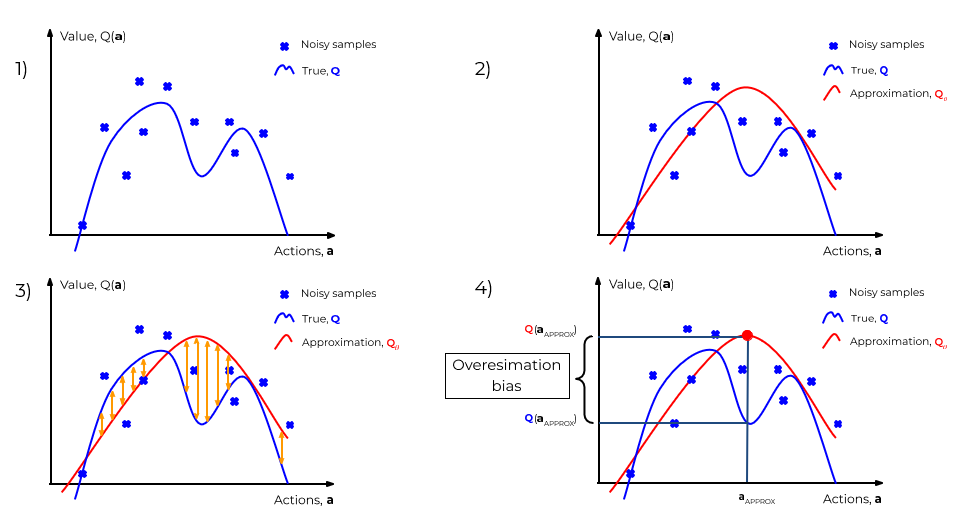
# 1. 强化学习中的损失函数基础
强化学习(Reinforcement Learning, RL)是机器学习领域的一个重要分支,它通过与环境的互动来学习如何在特定任务中做出决策。在强化学习中,损失函数(loss function)起着至关重要的作用,它是学习算法优化的关键所在。损失函数能够衡量智能体(agent)的策略(policy)表现,帮助智能体通过减少损失来改进自
在Flow-3D中,如何根据水利工程的特定需求设定边界条件和进行网格划分,以便准确模拟水流问题?
在Flow-3D中模拟水利工程时,设定正确的边界条件和精确的网格划分对于得到准确的模拟结果至关重要。具体步骤包括:
参考资源链接:[Flow-3D水利教程:边界条件设定与网格划分](https://wenku.csdn.net/doc/23xiiycuq6?spm=1055.2569.3001.10343)
1. **边界条件设定**:确定模拟中流体的输入输出位置。例如,在模拟渠道流时,可能需要设定上游入口(Inlet)边界条件,提供入口速度或流量信息,以及下游出口(Outlet)边界条件,设定压力或流量。对于开放水体,可能需要设置壁面(Wall)边界条件,以模拟水体与结构物的相互
Python实现8位等离子效果开源项目plasma.py解读
资源摘要信息:"plasma.py是一个开源的Python项目,旨在实现8位等离子效果。它基于Alex Champandard的C++代码,并对其进行了端口移植。等离子效果是一种视觉效果,类似于老式电视机的雪花屏,或者老旧计算机显示器的故障显示,它通过动态变化的彩色图案来模拟。在现代计算机图形学中,等离子效果常用于游戏和媒体艺术中,以创造复古或科幻的视觉体验。"
"plasma.py项目使用了pygame模块,这是Python的一个跨平台的模块,专为电子游戏设计,包括图形和声音库。在plasma.py中,pygame被用来处理绘图和屏幕更新,允许开发者在Python环境中轻松实现动态的图形效果。该模块的使用简化了编程过程,因为它提供了一个直观的API来控制渲染循环、声音播放以及其他相关的游戏开发功能。"
"该代码示例的特别之处在于,它是Alex Champandard所编写C++代码的一个端口版本。Alex Champandard是一位在人工智能和游戏开发领域有广泛影响的开发者。他的C++代码具有高效且精确的特点,因此被广泛应用于图形处理和游戏开发中。将其转换为Python版本,使得更多的开发者能够使用这一技术,特别是那些更熟悉Python而不是C++的开发者。"
"此项目为开源软件,意味着源代码是可访问的,并且开发者可以自由地使用、修改和重新分发软件及其源代码。开源软件鼓励社区参与和协作,促进了技术的共享和创新。在这样一个开放的环境中,plasma.py可以不断地改进和扩展,为其他开发者提供灵感,并在不断增长的开源生态系统中发挥其作用。"
"文件名称中的'plasma-1.4_win_src'暗示了这是一个Windows平台上的源代码文件,版本号为1.4。这表明该文件是为Windows操作系统设计的源代码包,包含了完整的源代码文件,开发者可以使用它来编译和运行等离子效果程序。这同样表明,尽管是开源软件,该项目仍然注重于特定平台的用户,使其能够更容易地参与到软件的使用和开发中来。"
"除了为开发者提供了一个有趣和富有创意的方式来学习和实践图形编程之外,plasma.py还展示了如何将复杂的效果代码从一种编程语言转换到另一种语言,这对学习编程语言间的差异和各自的特性非常有帮助。这对于任何希望深化其编程知识的开发者来说,都是一个宝贵的学习资源。"