
Page 4 of 18
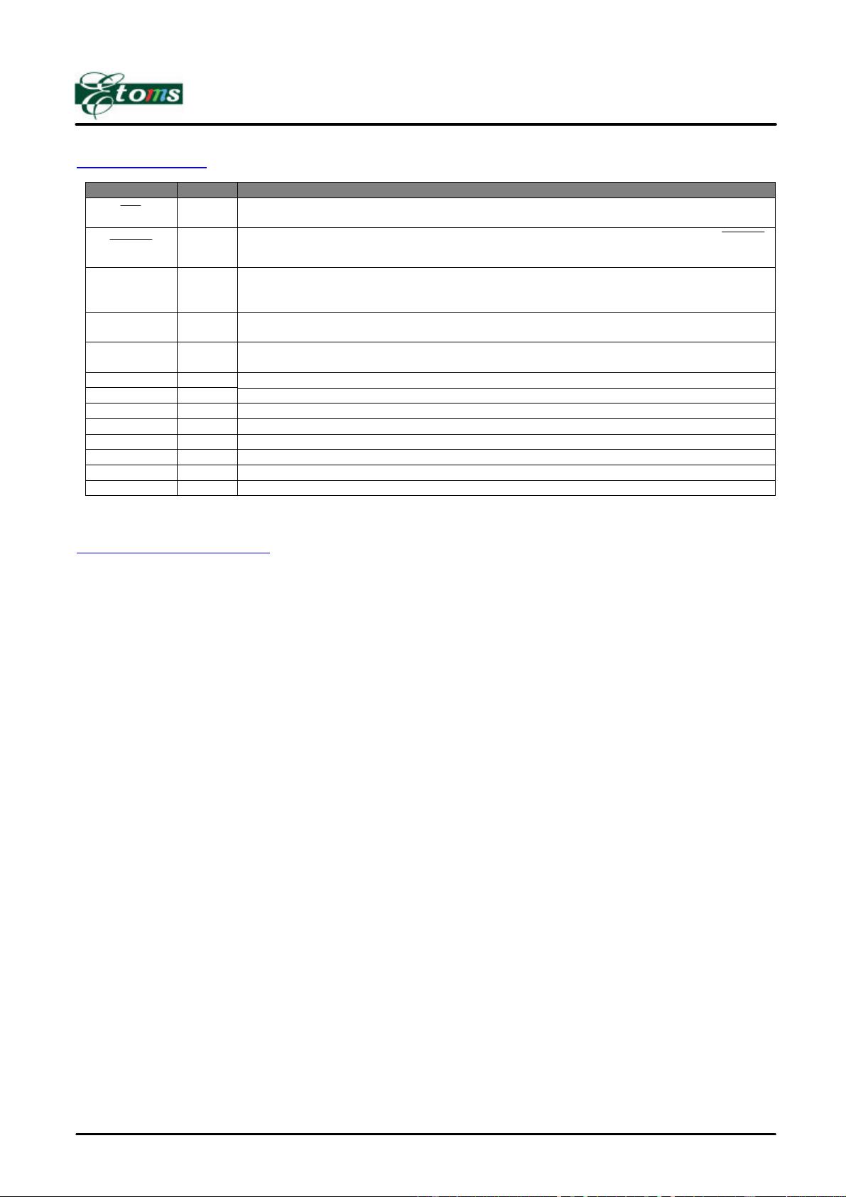
Pin Description
Symbol Type Description
EA
I
EXTERIAL ACCESS ENABLE: This pin should be forced to high level and the program
counter is within the 64 KB area.
PSEN
O/H
PROGRAM STORE ENABLE: When internal ROM access is performed, no
PSEN
strobe signal output is originated from this pin.
ALE O/H
ADDRESS LATCH ENABLE: ALE is used to enable the address latch that separates the
address from the data on Port 0. ALE runs at 1/6
th
of the oscillator frequency. An ALE
pulse is omitted during external data memory accesses.
RST I/L
RESET: A high on this pin for two machine cycles resets the device while the oscillator is
running.
XTAL1 I
CRYSTAL 1: This is the crystal oscillator input. The pin may be driven by an external
clock.
XTAL2 O CRYSTAL 2: This is the crystal oscillator output. It is the inversion of XTAL1.
V
SS
I GROUND: Ground potential.
V
DD
I POWER SUPPLY: Supply voltage for operation.
P0.0 - P0.7 I/O/D PORT 0: Function is the same as that of standard 8051.
P1.0 - P1.7 I/O/H PORT 1: Function is the same as that of standard 8051.
P2.0 - P2.7 I/O/H PORT 2: Function is the same as that of standard 8051.
P3.0 - P3.7 I/O/H PORT 3: Function is the same as that of standard 8051.
P4.0 - P4.3 I/O/H PORT 4: A bi-directional I/O port with internal pull-ups.
NOTES: TYPE I: input; O: output; I/O: bi-directional; H: pull-high; L: pull-low; D: open drain.
Functional Description
The ET45M052 architecture consists of a core controller
surrounded by various registers, four general-purpose
I/O port, 512-byte RAM, three timer/counters, a serial
port. Its processor supports 111 different opcodes
and references, both 64K program address space and
64K data storage space.
RAM
The internal data RAM of ET45M052 has 512 bytes and
is divided into two banks: scratchpad 256-byte RAM
and 256-byte AUX-RAM. These RAMs are
addressed by different ways:
RAM 00H-7FH can be addressed directly and
indirectly as the same as in 8051. Address
pointers are R0 and R1 of the selected register
bank.
RAM 80H-FFH can only be addressed indirectly
as the same as in 8051. Address pointers are
R0 and R1 of the selected registers bank.
AUX-RAM 00H-FFH is addressed indirectly as
the same way to access external data memory
with the MOVX instruction. Address pointers
are R0 and R1 of the selected register bank and
DPTR register. The AUX-RAM is disabled
after a reset. Setting the bit 4 in CHPCON
register will enable the access to on-chip
AUX-RAM.
Timers 0, 1, and 2
Timers 0, 1, and 2 each consist of two 8-bit data
registers. These are called TL0 and TH0 for Timer 0,
TL1 and TH1 for Timer 1, and TL2 and TH2 for Timer
2. The TCON and TMOD registers provide control
functions for timers 0 and 1. The T2CON register
provides control functions for Timer 2. RCAP2H and
RCAP2L are used as auto-reload or capture registers
for Timer 2 as it in 8051.
The operations of Timer 0 and Timer 1 are the same
as the standard 8051. Timer 2 is a 16-bit
timer/counter that is configured and controlled by the
T2CON register. Like timers 0 and 1, Timer 2 can
operate as either an external event counter or as an
internal timer, depending on the setting of bit C/T2 in
T2CON. Timer 2 has three operating modes:
capture, auto-reload, and baud rate generator. The
clock speed at capture or auto-reload mode is the
same as that of timers 0 and 1.
8051 MICROCONTROLLER WITH 8K FLASH AND ISP
ET45M052
剩余17页未读,继续阅读

tianxiao131420
- 粉丝: 0
- 资源: 3
 我的内容管理
展开
我的内容管理
展开


最新资源
- C++多态实现机制详解:虚函数与早期绑定
- Java多线程与异常处理详解
- 校园导游系统:无向图实现最短路径探索
- SQL2005彻底删除指南:避免重装失败
- GTD时间管理法:提升效率与组织生活的关键
- Python进制转换全攻略:从10进制到16进制
- 商丘物流业区位优势探究:发展战略与机遇
- C语言实训:简单计算器程序设计
- Oracle SQL命令大全:用户管理、权限操作与查询
- Struts2配置详解与示例
- C#编程规范与最佳实践
- C语言面试常见问题解析
- 超声波测距技术详解:电路与程序设计
- 反激开关电源设计:UC3844与TL431优化稳压
- Cisco路由器配置全攻略
- SQLServer 2005 CTE递归教程:创建员工层级结构
资源上传下载、课程学习等过程中有任何疑问或建议,欢迎提出宝贵意见哦~我们会及时处理!
点击此处反馈


