
number of multiplexers for efficient comparison which
increases the area overhead and power.
Time-delay PUF [32–35] leverages multiple delay stages
consisting of two RC race paths, where a multiplexer tailors
the delay paths depending on the selector bits. It also employs
an arbiter which generates a bit depending on the delay path
that won the race. RC values in time delay based PUF is
sensitive to temperature and supply voltage fluctuations thus
making the reliability (intra-hamming distance ) a concern.
Memory based PUFs that utilize- inverter mismatch and
threshold voltage variability in SRAM cells [36–39], meta-
stable states in buskeeper, latches or D flip-flops [40–42], and
even the program/read disturbance in FLASH memories
[43, 44] have also been proposed. While SRAM based
solutions offer low density, FLASH based PUF is subject to
bit errors. Furthermore, conventional CMOS based PUFs
often require an error correction hardware such as fuzzy
extractor as a post-processing unit to stabilize the response
string and enhance the entropy. The fuzzy extractor uses
helper data which may be vulnerable to partial leak of
information thus making the PUF prone to attacks.
In this context, several new hybrid hardware (i.e.
CMOS+emerging Non Volatile Memory (NVM)) [45–67],
security solutions (PUF/RNG) have emerged recently. These
promise low silicon footprint, ease of integration, exploitation
of undesirable nanoscale device phenomena, and added
benefit of high-density on-chip NVM.
In this paper, we provide a comprehensive review of
RNG/PUF implementations speci fically based on emerging
resistive NVM devices. The field is attracting increased
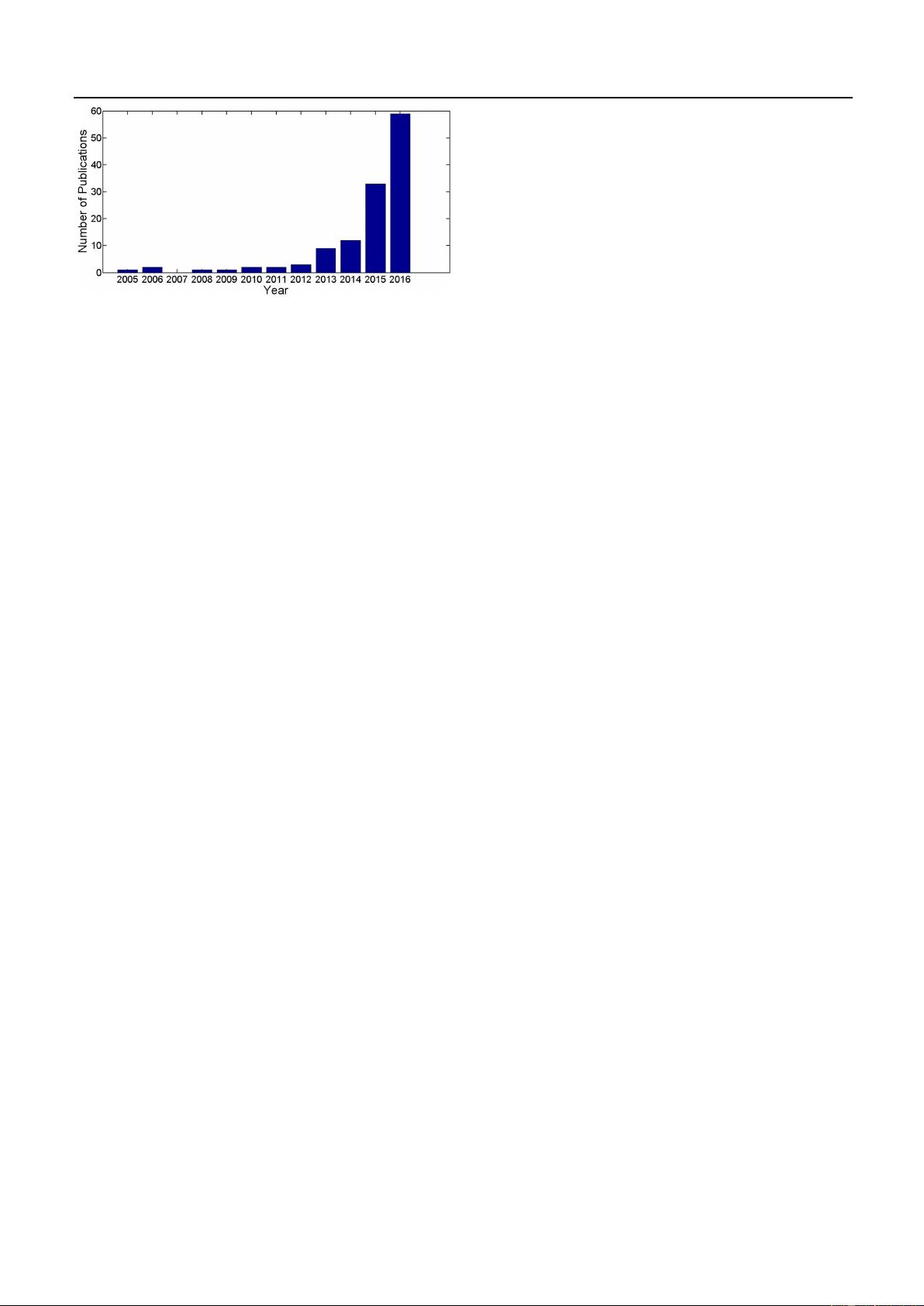
attention and steadily growing (see figure 1). The present
review serves as an advanced tutorial for state-of-the art, and
attempts to provide qualitative benchmarking of cross-tech-
nology RNG/PUF implementations, that might help readers
make informed design choices.
The review is organized as follows: section 2 briefly
explains the basics of resistive oxide based (OxRAM), and
magneto-resistive spin based (STT-MRAM) emerging NVM
devices. It also discusses different experimentally observed
undesirable variability/stochasticity phenomena exploited for
the application of interest. Section 3 presents a detailed
comparative discussion of various recent hybrid CMOS-
NVM circuits and approaches for RNG/PUF applications,
followed by the Conclusion.
2. Properties of emerging resistive NVM devices
2.1. Basic working principle
Two major categories of emerging NVM devices include the
resistive switching based (RRAM), and magneto-resistive
switching based (STT-MRAM) devices. Most RRAM devices
are two-terminal MIM (metal-insulator-metal) structures
where an insulating layer, sandwiched between two metal
electrodes (figure 2(a)), exhibits reversible non-volatile
switching depending on the applied programming voltage/
current across the electrodes. If the active switching insulator
layer is a metal oxide such as HfOx, AlOx, TiOx, TaOx etc,
the device may be further classified as OxRAM. In certain
cases the sandwiched insulating layer is a solid electrolyte
such as GeS
2
, with a sacrificial top electrode ( Ag/Cu ),
leading to a programmable metallization cell (PMC) also
known as CBRAM (conductive bridge).Infilamentary
OxRAM devices, formation of a conductive filament (CF)
consisting of oxygen vacancies and defects in the insulator
layer leads the device to a low-resistance (LRS) state, while
the dissolution of the filament results in a high-resistance
(HRS) state, as shown in figure 2(a). In CBRAM/PMC
devices the CF is formed/dissolved owing to an electro-
chemical redox reaction where ions of the sacrificial top
electrode metal layer plays a pivotal role.
Magneto-resistive switching based devices exploit the
tunnel magneto resistance (TMR) effect of magnetic tunnel
junction (MTJ) which is a three-layered stack. A thin oxide
barrier layer (like MgO) is sandwiched between a fixed and a
free magnetic layer (generally CoFeB) in a typical MTJ
(figure 2(b)). The fixed layer has a pre-defined magnetization
state while the magnetization state of the free layer can be
perturbed using a current pulse. When programming current
flows through the fixed layer, electrons become spin polarized
according to spin of the fixed layer. When such stream of spin
polarized electrons enters the free layer, it changes the
magnetic state of the free layer. Therefore, the application of
programming current pulse changes the magnetic state of the
magnetic free layer in the MTJ leading to a spin-transfer-
torque based switching. In STT-MRAM, the low resistance
state corresponds to P
(parallel) spin orientation of both fixed
and free layers. High resistance state corresponds to AP (Anti-
parallel) spin orientation of the free and fixed layer
(figure 2(b)). The TMR ratio is defined as: TMR=(R
AP
−
R
P
)/R
P
. A high TMR ratio denotes larger resistance window
and is favorable for memory application.
2.2. Undesirable effects (variability/stochasticity) and
underlying physics
Undesirable device variability/stochasticity phenomena exist
either as temporal (intrinsic, cycle-to-cycle (C2C)), or spatial
Figure 1. Recent publication trend in the field of hardware security
using emerging NVM devices. Statistics obtained from web of
science using all combinations of keywords (X AND Y), where
X={RNG, PUF} and Y={RRAM, ReRAM, OxRAM, MTJ,
CBRAM, PCM, STT-MRAM, memristor}.
3
Semicond. Sci. Technol. 32 (2017) 123001 Topical Review
剩余17页未读,继续阅读

元辰辰辰辰辰辰
- 粉丝: 55
- 资源: 76
 我的内容管理
展开
我的内容管理
展开


最新资源
- AirKiss技术详解:无线传递信息与智能家居连接
- Hibernate主键生成策略详解
- 操作系统实验:位示图法管理磁盘空闲空间
- JSON详解:数据交换的主流格式
- Win7安装Ubuntu双系统详细指南
- FPGA内部结构与工作原理探索
- 信用评分模型解析:WOE、IV与ROC
- 使用LVS+Keepalived构建高可用负载均衡集群
- 微信小程序驱动餐饮与服装业创新转型:便捷管理与低成本优势
- 机器学习入门指南:从基础到进阶
- 解决Win7 IIS配置错误500.22与0x80070032
- SQL-DFS:优化HDFS小文件存储的解决方案
- Hadoop、Hbase、Spark环境部署与主机配置详解
- Kisso:加密会话Cookie实现的单点登录SSO
- OpenCV读取与拼接多幅图像教程
- QT实战:轻松生成与解析JSON数据
资源上传下载、课程学习等过程中有任何疑问或建议,欢迎提出宝贵意见哦~我们会及时处理!
点击此处反馈


