
6.6 Insulation Specifications
over operating ambient temperature range (unless otherwise noted)
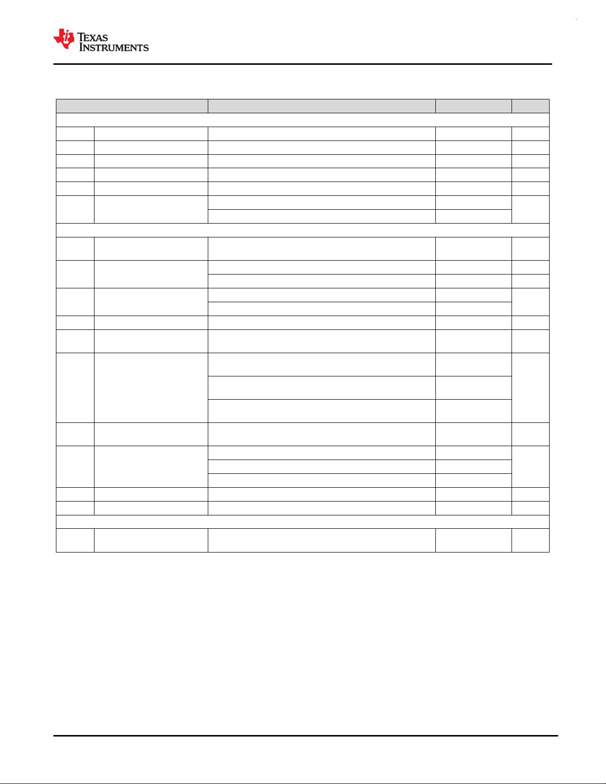
PARAMETER TEST CONDITIONS VALUE UNIT
GENERAL
CLR External clearance
(1)
Shortest pin-to-pin distance through air ≥ 4 mm
CPG External creepage
(1)
Shortest pin-to-pin distance across the package surface ≥ 4 mm
DTI Distance through insulation Minimum internal gap (internal clearance) of the insulation ≥ 15.4 µm
CTI Comparative tracking index DIN EN 60112 (VDE 0303-11); IEC 60112 ≥ 400 V
Material group According to IEC 60664-1 II
Overvoltage category
per IEC 60664-1
Rated mains voltage ≤ 150 V
RMS
I-IV
Rated mains voltage ≤ 300 V
RMS
I-III
DIN EN IEC 60747-17 (VDE 0884-17)
(2)
V
IORM
Maximum repetitive peak
isolation voltage
At AC voltage 790 V
PK
V
IOWM
Maximum-rated isolation
working voltage
At AC voltage (sine wave) 560 V
RMS
At DC voltage 790 V
DC
V
IOTM
Maximum transient
isolation voltage
V
TEST
= V
IOTM
, t = 60 s (qualification test) 4250
V
PK
V
TEST
= 1.2 × V
IOTM
, t = 1 s (100% production test) 5100
V
IMP
Maximum impulse voltage
(3)
Tested in air, 1.2/50-µs waveform per IEC 62368-1 5000 V
PK
V
IOSM
Maximum surge
isolation voltage
(4)
Tested in oil (qualification test),
1.2/50-µs waveform per IEC 62368-1
6500 V
PK
q
pd
Apparent charge
(5)
Method a, after input/output safety test subgroups 2 and 3,
V
ini
= V
IOTM
, t
ini
= 60 s, V
pd(m)
= 1.2 × V
IORM
, t
m
= 10 s
≤ 5
pC
Method a, after environmental tests subgroup 1,
V
ini
= V
IOTM
, t
ini
= 60 s, V
pd(m)
= 1.3 × V
IORM
, t
m
= 10 s
≤ 5
Method b2, at routine test (100% production),
V
ini
= V
IOTM
= V
pd(m)
; t
ini
= t
m
= 1 s
≤ 5
C
IO
Barrier capacitance,
input to output
(6)
V
IO
= 0.5 V
PP
at 1 MHz ~1 pF
R
IO
Insulation resistance,
input to output
(6)
V
IO
= 500 V at T
A
= 25°C > 10
12
ΩV
IO
= 500 V at 100°C ≤ T
A
≤ 125°C > 10
11
V
IO
= 500 V at T
S
= 150°C > 10
9
Pollution degree 2
Climatic category 55/125/21
UL1577
V
ISO
Withstand isolation voltage
V
TEST
= V
ISO
= 3000 V
RMS
or 4250 V
DC
, t = 60 s (qualification),
V
TEST
= 1.2 × V
ISO
= 3600 V
RMS
, t = 1 s (100% production test)
3000 V
RMS
(1) Apply creepage and clearance requirements according to the specific equipment isolation standards of an application. Care must be
taken to maintain the creepage and clearance distance of a board design to ensure that the mounting pads of the isolator on the
printed circuit board (PCB) do not reduce this distance. Creepage and clearance on a PCB become equal in certain cases. Techniques
such as inserting grooves, ribs, or both on a PCB are used to help increase these specifications.
(2) This coupler is suitable for safe electrical insulation only within the safety ratings. Compliance with the safety ratings shall be ensured
by means of suitable protective circuits.
(3) Testing is carried out in air to determine the surge immunity of the package.
(4) Testing is carried out in oil to determine the intrinsic surge immunity of the isolation barrier.
(5) Apparent charge is electrical discharge caused by a partial discharge (pd).
(6) All pins on each side of the barrier are tied together, creating a two-pin device.
www.ti.com
AMC22C12
SBASAJ8 – JUNE 2022
ADVANCE INFORMATION
Copyright © 2022 Texas Instruments Incorporated
Submit Document Feedback
7
Product Folder Links: AMC22C12
剩余34页未读,继续阅读

不觉明了
- 粉丝: 3278
- 资源: 5614
 我的内容管理
收起
我的内容管理
收起
- 我的资源
快来上传第一个资源
 我的收益 登录查看自己的收益
 我的积分
登录查看自己的积分
我的积分
登录查看自己的积分
 我的C币
登录后查看C币余额
我的C币
登录后查看C币余额
 我的收藏
我的收藏  我的下载
我的下载  下载帮助
下载帮助

会员权益专享


最新资源
- 谷歌文件系统下的实用网络编码技术在分布式存储中的应用
- 跨国媒体对南亚农村社会的影响:以斯里兰卡案例的社会学分析
- RFM2g接口驱动操作手册:API与命令行指南
- 基于裸手的大数据自然人机交互关键算法研究
- ABAQUS下无人机机翼有限元分析与局部设计研究
- TCL基础教程:语法、变量与操作详解
- FPGA与数字前端面试题集锦:流程、设计与Verilog应用
- 2022全球互联网技术人才前瞻:元宇宙驱动下的创新与挑战
- 碳排放权交易实战手册(第二版):设计与实施指南
- 2022新经济新职业洞察:科技驱动下的百景变革
- 红外与可见光人脸融合识别技术探究
- NXP88W8977:2.4/5 GHz 双频 Wi-Fi4 + Bluetooth 5.2 合体芯片
- NXP88W8987:集成2.4/5GHz Wi-Fi 5与蓝牙5.2的单芯片解决方案
- TPA3116D2DADR: 单声道数字放大器驱动高达50W功率
- TPA3255-Q1:315W车载A/D类音频放大器,高保真、宽频设计
- 42V 输入 5A 降压稳压器 TPS54540B-Q1 的特点和应用
资源上传下载、课程学习等过程中有任何疑问或建议,欢迎提出宝贵意见哦~我们会及时处理!
点击此处反馈


