"TI-DS110DF111.pdf: 以太网重定时器设计与接口指南"
82 浏览量
更新于2023-12-20
4
收藏 1.34MB PDF 举报
TI-DS110DF111.pdf is a datasheet for the DS110DF111, an Ethernet retimer chip designed to improve signal integrity in high-speed networking applications. The chip features VDDOUTA and POUTA_N, as well as INB_PINB and NSCLADDR0/LOCKSDAINA_PINA_NOUTB_POUTB_N. In addition, the datasheet provides details on the recommended power supply configuration, including the use of 100nF and 25 MHz components. The DS110DF111 operates at a voltage of 3.3V and has a capacitance of 0.22μF (2x). The datasheet also outlines the pin assignments, including REFCLK_INEN_SMBGND and various 1kΩ and 2kΩ components. Additionally, the datasheet includes information on ADDR1/VODB/DONE and other key features of the DS110DF111.
In conclusion, the TI-DS110DF111.pdf datasheet provides comprehensive information on the DS110DF111 Ethernet retimer chip, including its key features, pin assignments, power supply recommendations, and other important details for designers and engineers working on high-speed networking applications.
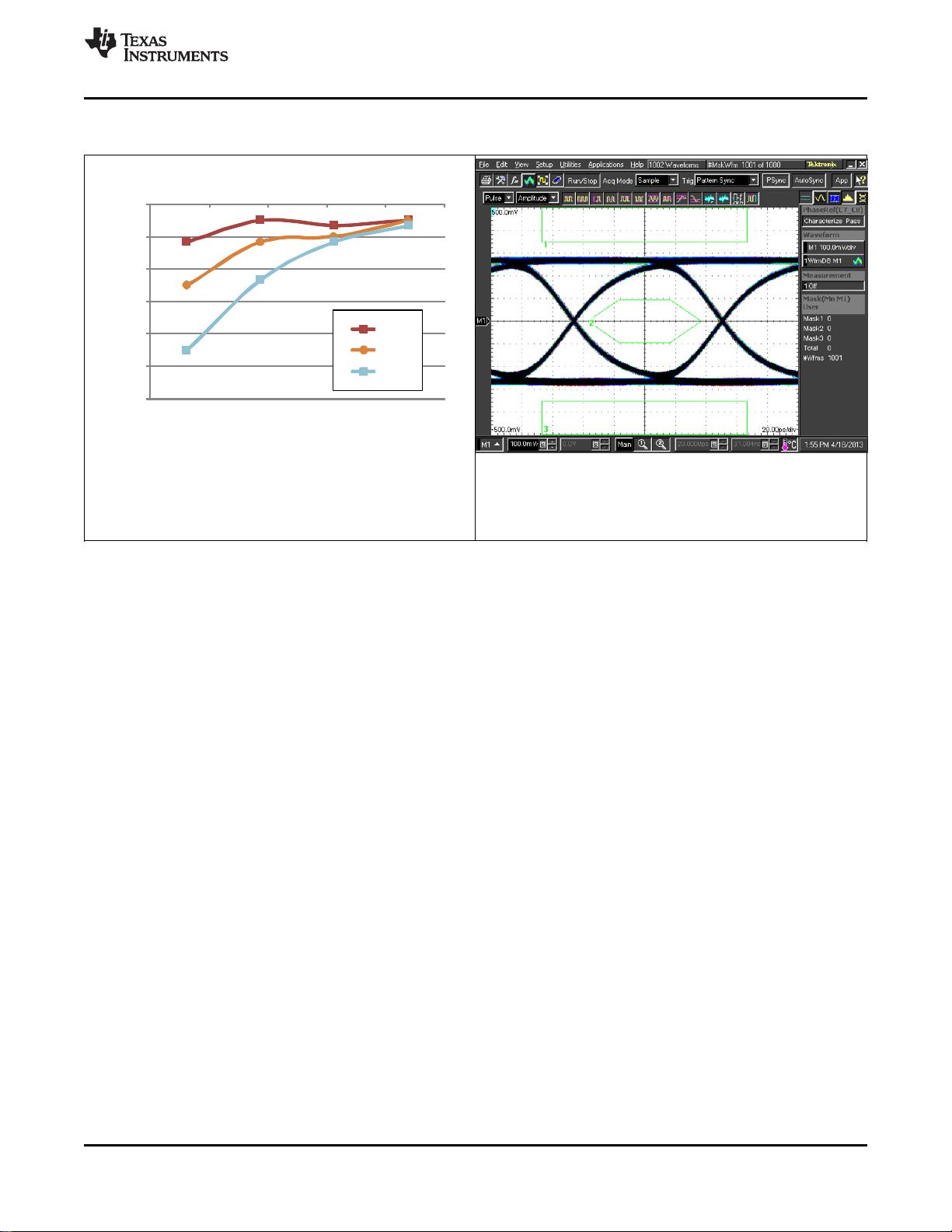
Frequency (MHz)
-6
-5
-4
-3
-2
-1
0
0 1000 2000 3000 4000 5000
-1.5
-3.5
-6
De-Emphasis (dB)
DS110DF111
www.ti.com.cn
ZHCSDW7A –MAY 2013–REVISED JUNE 2015
6.6 Typical Characteristics
Test Conditions
Datarate: 10.3125 Gbps with a PRBS7 pattern
Jitter Measurements
VOD Setting: 1000mV
Rj (RMS): 315 fs Dj: 3.74 ps Tj (1E-12): 7.33 ps
Temperature: 25°C and VDD = 2.5V
Figure 5. Output Eye Diagram 10.3125 Gbps
Figure 4. De-Emphasis Gain vs. Frequency
Copyright © 2013–2015, Texas Instruments Incorporated 9

剩余52页未读,继续阅读
2022-12-16 上传
点击了解资源详情
点击了解资源详情
点击了解资源详情
点击了解资源详情
论文
点击了解资源详情
论文
2023-05-26 上传

不觉明了
- 粉丝: 3436
- 资源: 5759
 我的内容管理
展开
我的内容管理
展开


最新资源
- OptiX传输试题与SDH基础知识
- C++Builder函数详解与应用
- Linux shell (bash) 文件与字符串比较运算符详解
- Adam Gawne-Cain解读英文版WKT格式与常见投影标准
- dos命令详解:基础操作与网络测试必备
- Windows 蓝屏代码解析与处理指南
- PSoC CY8C24533在电动自行车控制器设计中的应用
- PHP整合FCKeditor网页编辑器教程
- Java Swing计算器源码示例:初学者入门教程
- Eclipse平台上的可视化开发:使用VEP与SWT
- 软件工程CASE工具实践指南
- AIX LVM详解:网络存储架构与管理
- 递归算法解析:文件系统、XML与树图
- 使用Struts2与MySQL构建Web登录验证教程
- PHP5 CLI模式:用PHP编写Shell脚本教程
- MyBatis与Spring完美整合:1.0.0-RC3详解
