
ULN2003LV
ZHCS846B –APRIL 2012–REVISED JUNE 2015
www.ti.com.cn
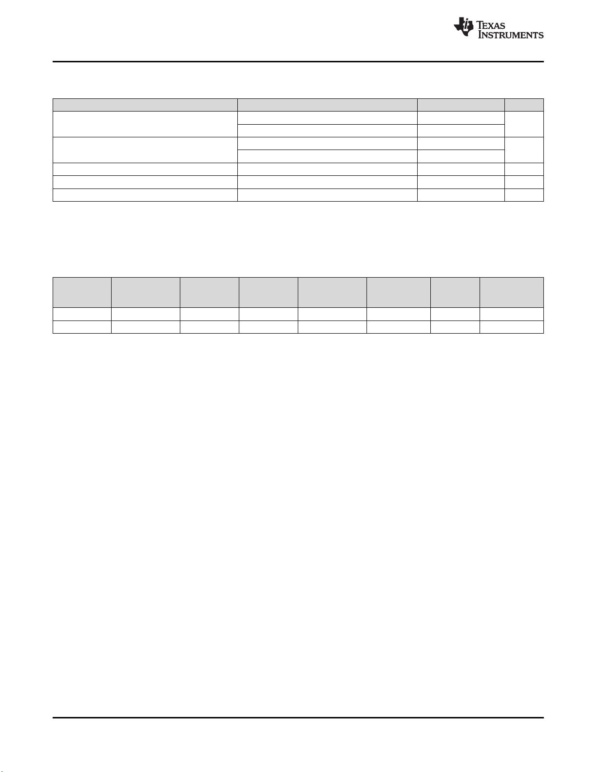
6.6 Switching Characteristics
over operating free-air temperature range (unless otherwise noted)
(1)(2)
PARAMETER TEST CONDITIONS MIN TYP MAX UNIT
V
INX
= 3.3V, V
pull-up
= 3.3 V, R
pull-up
= 50 Ω 25
OUT1–OUT7 logic high propagation
t
PHL
ns
delay
V
INX
= 5.0V, V
pull-up
= 5 V, R
pull-up
= 1 kΩ 15
V
INX
= 3.3V, V
pull-up
= 3.3 V, R
pull-up
= 50 Ω 45
t
PLH
OUT1–OUT7 logic low propagation delay ns
V
INX
= 5.0V, V
pull-up
= 5 V, R
pull-up
= 1kΩ 80
R
PD
IN1–IN7 input pull-down Resistance 210 300 390 kΩ
ζ IN1–IN7 Input filter time constant 9 ns
C
OUT
OUT1–OUT7 output capacitance V
INX
= 3.3 V, V
OUTX
= 0.4 V 15 pF
(1) Rise and Fall propagation delays, t
PHL
and t
PLH
, are measured between 50% values of the input and the corresponding output signal
amplitude transition.
(2) Specified by design only.
6.7 Dissipation Ratings
See
(1)(2)
DERATING
BOARD PACKAGE R
θJC
R
θJA
(3)
FACTOR ABOVE T
A
< 25°C T
A
= 70°C T
A
= 85°C
T
A
= 25ºC
High-K 16-Pin SOIC 69°C/W 112°C/W 8.88 mW/ºC 1.11 W 0.71 W 0.58 W
High-K 16-Pin TSSOP 74°C/W 142°C/W 7.11 mW/ºC 0.88 W 0.56 W 0.45 W
(1) Maximum dissipation values for retaining device junction temperature of 150°C
(2) Refer to TI’s design support web page at www.ti.com/thermal for improving device thermal performance
(3) Operating at the absolute T
J-max
of 150°C can affect reliability– for higher reliability it is recommended to ensure T
J
< 125°C
6 Copyright © 2012–2015, Texas Instruments Incorporated
剩余28页未读,继续阅读

不觉明了
- 粉丝: 3278
- 资源: 5614
 我的内容管理
收起
我的内容管理
收起
- 我的资源
快来上传第一个资源
 我的收益 登录查看自己的收益
 我的积分
登录查看自己的积分
我的积分
登录查看自己的积分
 我的C币
登录后查看C币余额
我的C币
登录后查看C币余额
 我的收藏
我的收藏  我的下载
我的下载  下载帮助
下载帮助

会员权益专享


最新资源
- 谷歌文件系统下的实用网络编码技术在分布式存储中的应用
- 跨国媒体对南亚农村社会的影响:以斯里兰卡案例的社会学分析
- RFM2g接口驱动操作手册:API与命令行指南
- 基于裸手的大数据自然人机交互关键算法研究
- ABAQUS下无人机机翼有限元分析与局部设计研究
- TCL基础教程:语法、变量与操作详解
- FPGA与数字前端面试题集锦:流程、设计与Verilog应用
- 2022全球互联网技术人才前瞻:元宇宙驱动下的创新与挑战
- 碳排放权交易实战手册(第二版):设计与实施指南
- 2022新经济新职业洞察:科技驱动下的百景变革
- 红外与可见光人脸融合识别技术探究
- NXP88W8977:2.4/5 GHz 双频 Wi-Fi4 + Bluetooth 5.2 合体芯片
- NXP88W8987:集成2.4/5GHz Wi-Fi 5与蓝牙5.2的单芯片解决方案
- TPA3116D2DADR: 单声道数字放大器驱动高达50W功率
- TPA3255-Q1:315W车载A/D类音频放大器,高保真、宽频设计
- 42V 输入 5A 降压稳压器 TPS54540B-Q1 的特点和应用
资源上传下载、课程学习等过程中有任何疑问或建议,欢迎提出宝贵意见哦~我们会及时处理!
点击此处反馈


