没有合适的资源?快使用搜索试试~ 我知道了~
首页Reliability of 3D NAND Flash Memories
资源详情
资源推荐
Chapter 2
Reliability of 3D NAND Flash Memories
A. Grossi, C. Zambelli and P. Olivo
2.1 Introduction
Reliability represents one of the major antagonist towards the unstoppable tech-
nological evolution of hyperscaled NAND memories, since the correct operations
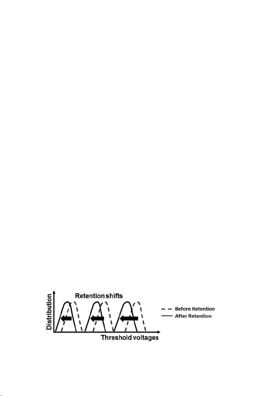
must be assured throughout the entire lifetime. In particular, the ability of keeping
unaltered the stored information even after a consistent number of write operations
and for long times must be guaranteed.
A growth of the memory devices storage capacity without increasing the area
occupation is constantly requested by the market: in order to sati sfy such require-
ments, an increase of the memory density and of cell shrinking is mandatory.
Nowadays, the transition from planar to three-dimensional architectures appears as
the most viable solution for the integration of non-volatile memory cells in Tera-bit
arrays. Charge Trap (CT) NAND memory cells are considered as one of the most
promising technology for 3D integration because of a better scalability than
Floating Gate (FG) NAND. Despite the high theoretical potentialities demonstrated
by CT memories, several reliability issues affect such technology. Moreover, the
transition from 2D to 3D changed the impact of the previously known reliability
issues and generated new problems. Recently, in order to overcome such problems,
new 3D vertical FG type NAND cell arrays have been proposed with promising
performances.
A. Grossi (&) C. Zambelli P. Olivo
Dipartimento di Ingegneria, Università degli Studi di Ferrara, Ferrara, Italy
e-mail: alessandro.grossi@unife.it
C. Zambelli
e-mail: cristian.zambelli@unife.it
P. Olivo
e-mail: piero.olivo@unife.it
© Springer Science+Business Media Dordrecht 2016
R. Micheloni (ed.), 3D Flash Memories, DOI 10.1007/978-94-017-7512-0_2
29
In this chapter the main reliability mechanisms affecting 3D NAND memories
will be addressed, providing a comparison between 3D FG and 3D CT devices in
terms of reliability and expected performances. Starting from an analysis of basic
reliability issues related to both physical and architectural aspects affecting NAND
memories, the specific physical mechanisms impacting the reliability of 2D
CT NAND will be addressed. Then, a review of the main problems experimentally
observed in different 3D CT cell concepts is reported. Finally, 3D FG memory
concept is briefly introduced in order to understand the related reliability implica-
tions, and a comparison between 3D CT and 3D FG arrays is provided in terms of
reliability and expected performances.
2.2 NAND Flash Reliability
During its lifetime a NAND Flash module undergoes a large number of
Program/Erase (P/E) cycles. Every cycle involves very high electric fields applied to
the tunnel oxide. The reliability of the entire memory requires that the tunnel oxide is
able to correctly operate under stress conditions. It is obvious that huge efforts are to
be spent to determine the right process for the tunnel oxide creation (in terms of
thickness, material, growth, defectivity, interface, …) and the most effective algo-
rithms in order to achieve a successful and reliable NAND technology.
In this section we will analyze the basic physical mechanisms related to the
tunnel oxide, which affect both memory endurance and data retention. “Endurance”
of a memory module is defined as the minimum number of P/E cycles that the
module can withstand before leading to a failure. “Retention” is the ability of
storing the information over time even when the external power supply is not
applied. The tunnel oxide, which is a thin oxide, may be also responsible for other
effects, such as erratic bits and over-programming, which might induce read errors.
2.2.1 Endurance
In NAND flash cells, program and erase operations rely on charge transport through
thin oxides; this is accomplished via Fowler-Nordheim (FN) tunneling into/from a
storage layer, which can be either a polysilicon FG [1] or an interfacial trapping
layer in CT technology [2, 3]. Electron tunneling is responsible for a slow, but
continuous, oxide wear out because of traps creation and interfacial damages; as a
result, there might be charge trapping/detrapping into the tunneling oxide or
undesired charge flowing into/from the storage layer.
As the number of P/E cycles increases, the above mentioned effects strongly
impact writing operations. For instance, electron trapping reduces the tunneling
efficiency so that, under constant voltage and time conditions, the charge injected
into/from the storage layer decreases cycle after cycle.
30 A. Grossi et al.
To counteract “endurance” effects, all writing algorithms are based on a
sequence of program/erase pulses, each one followed by a verify operation. This
sequence proceeds until the expected amount of charge is correctly transferred
into/from the storage layer. As the number of P/E cycles increases, the program-
ming time is expected to reduce, whereas the erase time is expected to grow.
Without these write and verify algorithms (Chap. 3) it would be impossible to
control the actual amount of charge transferred into/from the storage layer and
Multi Level Cell (MLC) architectures would not exist [4].
Even if endurance is controlled by sophisticated (but slow and power consum-
ing) algorithms, traps creation, charge trapping/detrapping, and interface damages
still degrade the tunnel oxide. As a result, it gets really problematic to retain the
stored information for extremely long times, which, at the end of the day, is a basic
requirement of the non-volatile paradigm.
2.2.2 Data Retention
As mentioned in the previous section, the ability of keeping the stored information
unaltered for a long time, i.e. the charge trapped into the storage layer, is mandatory
for non-volatile memories. However, even with no bias applied, electron after
electron, charge loss can lead to a read failure: a programmed cell can be read as
erased if its threshold voltage (V
T
) shifts below 0 V in case of Single-Level-Cell
(SLC), or towards a lower threshold level with respect to the initial threshold
voltage in case of MLC programming [5].
The higher the number of P/E cycles the worse the retention is, as it can be
appreciated in Fig. 2.1, which shows how the cumulative V
T
distributions of MLC
programmed cells changes over time. Charge loss from the storage layer moves the
V
T
distributions towards lower values: the rigid shift of the cumulative V
T
distri-
butions is related to the oxide degradation and traps generation at the interface
between storage layer and tunnel layer. These traps may be responsible for charge
loss from the storage layer towards the silicon substrate. In fact, an empty trap,
suitably positioned within the oxide, can activate Trap Assisted Tunneling
(TAT) mechanisms characterized by a significantly higher tunnel probability with
Fig. 2.1 Threshold voltage shifts induced by retention
2 Reliability of 3D NAND Flash Memories 31
respect to a triangular barrier unmodified by the trap presence. Moreover, an
electron trapped inside the oxide during writing operations may be detrapped later
on, when the cell is read or even when the cell is not addressed. As a result, the
empty trap may enhance the TAT phenomenon (assu ming a positive charged trap)
and, in addition, it can increase the electron field at the storage layer-tunnel oxide
interface, thus raising the probability of electron tunneling. It is clear that these
mechanisms are strongly related to the oxide degradation and, therefore, data
retention gets shorter with the number of applied writing pulses. In the MLC case,
the cells programmed at higher V
T
are more prone to data retention issues.
2.2.3 Erratic Bits and Over-Programming
The Fowler-Nordheim (FN) tunneling mechanism for writing and erasing data in
NAND Flash has been used for several decades, demonstrating a sufficient level of
reliability.
Nevertheless, it has been found that anomalous FN tunneling currents can occur
in random periods of time, thus leading to significant variations of the threshold
voltage after the writing operation [6] (see Fig. 2.2). This phenomenon is known as
erratic bits.
In a NAND array, the presence of this phenomenon is detrimental for the per-
formances of the memory as the unpredictable increase of the cell’s threshold
voltage may eventually induce the over-programming issue. As shown in Fig. 2.3,
conductive cells featuring relatively large threshold voltage are erroneously read as
Fig. 2.2 Example of erratic behaviors in four flash cells. Cells threshold voltage V
T
plotted versus
the number of cycles exhibits RTN [6]
32 A. Grossi et al.
OFF if over-programmed, and they can electrically isolate the NAND string. Such
behavior generates read errors and consequ ent read throughput loss due to the
additional work done by the Er ror Correcting Codes (ECC) trying to repair the
failed bits.
Since erratic behaviors are intima tely related to the electron tunneling mecha-
nism, they can potentially affect all the cells of an array [6].
Anomalous tunneling has been related to the presence/abs ence of a cluster of
positive charges in the tunnel oxide that strongly affects the FN tunneling operation.
As a first approximation, erratic behaviors can, therefore, be described in terms of a
two level Random Telegraph Noise (RTN) affecting the threshold voltage during
cycling, in which the normal and the anomalous threshold voltage levels are the
result of the presence of a cluster of more than 2, or less than 3, positive charges in
the tunnel oxide, respectively [7 , 8].
2.3 Architecture Dependent Reliability Issues
Architectural solutions for memory operations may also affect the overall reliability,
by inducing errors and even cell failures [1]. The most common effects are the so
called “disturbs”, that can be interpreted as the influence of an operation performed
on a cell (Read or Write) on the charge content of a different cell.
Read disturbs are the most frequent source of disturbs in NAND architectures.
This kind of disturb may occur when reading many times the same cell without any
Fig. 2.3 Effect of an
over-programmed cell in a
NAND flash string. In normal
conditions the status of the
cell to be read (supposed to be
ON) is correctly detected,
since all other cells are driven
by a V
PASS
so that they
behave as ON pass transistors.
In the presence of an
over-programmed cell
(V
T
>V
PASS
), the current
flow through the string is
inhibited and the absence of
current is attributed to a
programmed status of the cell
to be read, thus producing a
read error [6]
2 Reliability of 3D NAND Flash Memories 33
剩余34页未读,继续阅读
sheng955
- 粉丝: 0
- 资源: 1
上传资源 快速赚钱
- 我的内容管理 收起
- 我的资源 快来上传第一个资源
- 我的收益 登录查看自己的收益
- 我的积分 登录查看自己的积分
- 我的C币 登录后查看C币余额
- 我的收藏
- 我的下载
- 下载帮助
会员权益专享
最新资源
- GO婚礼设计创业计划:技术驱动的婚庆服务
- 微信行业发展现状及未来发展趋势分析
- 信息技术在教育中的融合与应用策略
- 微信小程序设计规范:友好、清晰的用户体验指南
- 联鼎医疗:三级甲等医院全面容灾备份方案设计
- 构建数据指标体系:电商、社区、金融APP案例分析
- 信息技术:六年级学生制作多媒体配乐古诗教程
- 六年级学生PowerPoint音乐动画实战:制作配乐古诗演示
- 信息技术教学设计:特点与策略
- Word中制作课程表:信息技术教学设计
- Word教学:制作课程表,掌握表格基础知识
- 信息技术教研活动年度总结与成果
- 香格里拉旅游网设计解读:机遇与挑战并存
- 助理电子商务师模拟试题:设计与技术详解
- 计算机网络技术专业教学资源库建设与深圳IT产业结合
- 微信小程序开发:网络与媒体API详解
资源上传下载、课程学习等过程中有任何疑问或建议,欢迎提出宝贵意见哦~我们会及时处理!
点击此处反馈
安全验证
文档复制为VIP权益,开通VIP直接复制
信息提交成功