
TJA1043 All information provided in this document is subject to legal disclaimers. © NXP B.V. 2013. All rights reserved.
Product data sheet Rev. 3 — 24 April 2013 6 of 27
NXP Semiconductors
TJA1043
High-speed CAN transceiver
7.1.1 Normal mode
In Normal mode, the transceiver can transmit and receive data via the bus lines CANH
and CANL (see Figure 1
for the block diagram). The differential receiver converts the
analog data on the bus lines into digital data which is output to pin RXD. The slope of the
output signals on the bus lines is controlled and optimized in a way that guarantees the
lowest possible EME. The bus pins are biased to 0.5V
CC
(via R
i
). Pin INH is active, so
voltage regulators controlled by pin INH (see Figure 7
) will be active too.
7.1.2 Listen-only mode
In Listen-only mode, the transceiver’s transmitter is disabled, effectively providing a
transceiver listen-only feature. The receiver will still convert the analog bus signal on
pins CANH and CANL into digital data, available for output on pin RXD. As in Normal
mode, the bus pins are biased at 0.5V
CC
and pin INH remains active.
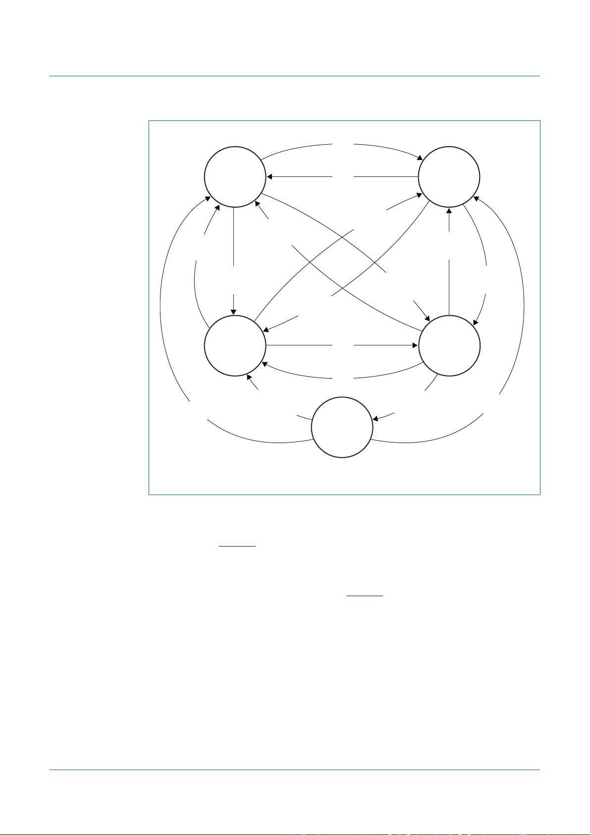
Fig 4. Mode transitions when valid V
CC
, V
IO
and V
BAT
voltages are present
015aaa063
STANDBY
MODE
NORMAL
MODE
GO-TO-SLEEP
MODE
LEGEND:
= H, = L logical state of pin
SLEEP
MODE
LISTEN-
ONLY MODE
Wake flag cleared
and
t > t
h(min)
STB_N = H and EN = H
STB_N = H and EN = L
STB_N = L
and
Wake flag set
STB_N = L
and
(EN = L or Wake flag set)
STB_N = L and EN = H
and
Wake flag cleared
STB_N = H
and
EN = H
STB_N = H
and
EN = L
STB_N = L
and
(EN = L or Wake flag set)
STB_N = L and EN = H
and
Wake flag cleared
STB_N = L
and
EN = H
STB_N = H
and
EN = H
STB_N = L
and
EN = L
STB_N = H
and
EN = L
STB_N = H
and
EN = H
STB_N = H
and
EN = L
剩余27页未读,继续阅读


