没有合适的资源?快使用搜索试试~ 我知道了~
首页PCA9555芯片资料
PCA9555芯片资料
4星 · 超过85%的资源 需积分: 48 76 下载量 101 浏览量
更新于2023-06-26
评论 1
收藏 203KB PDF 举报
PCA9555芯片资料,PCA9555用于IO口扩展,3.3V,可接5V
资源详情
资源评论
资源推荐
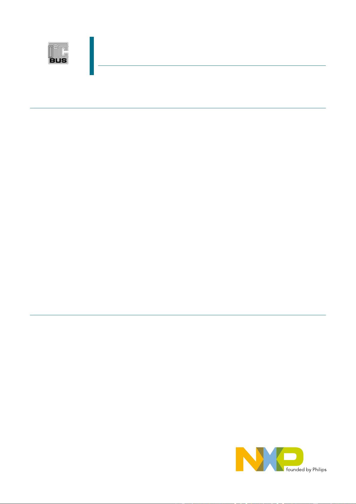
1. General description
The PCA9555 is a 24-pin CMOS device that provides 16 bits of General Purpose parallel
Input/Output (GPIO) expansion for I
2
C-bus/SMBus applications and was developed to
enhance the NXP Semiconductors family of I
2
C-bus I/O expanders. The improvements
include higher drive capability, 5 V I/O tolerance, lower supply current, individual I/O
configuration, and smaller packaging. I/O expanders provide a simple solution when
additional I/O is needed for ACPI power switches, sensors, push buttons, LEDs, fans, etc.
The PCA9555 consists of two 8-bit Configuration (Input or Output selection); Input, Output
and Polarity Inversion (active HIGH or active LOW operation) registers. The system
master can enable the I/Os as either inputs or outputs by writing to the I/O configuration
bits. The data for each Input or Output is kept in the corresponding Input or Output
register. The polarity of the read register can be inverted with the Polarity Inversion
register. All registers can be read by the system master. Although pin-to-pin and I
2
C-bus
address compatible with the PCF8575, software changes are required due to the
enhancements, and are discussed in
Application Note AN469
.
The PCA9555 open-drain interrupt output is activated when any input state differs from its
corresponding input port register state and is used to indicate to the system master that
an input state has changed. The power-on reset sets the registers to their default values
and initializes the device state machine.
Three hardware pins (A0, A1, A2) vary the fixed I
2
C-bus address and allow up to eight
devices to share the same I
2
C-bus/SMBus. The fixed I
2
C-bus address of the PCA9555 is
the same as the PCA9554, allowing up to eight of these devices in any combination to
share the same I
2
C-bus/SMBus.
2. Features
n Operating power supply voltage range of 2.3 V to 5.5 V
n 5 V tolerant I/Os
n Polarity Inversion register
n Active LOW interrupt output
n Low standby current
n Noise filter on SCL/SDA inputs
n No glitch on power-up
n Internal power-on reset
n 16 I/O pins which default to 16 inputs
n 0 Hz to 400 kHz clock frequency
n ESD protection exceeds 2000 V HBM per JESD22-A114, 200 V MM per
JESD22-A115, and 1000 V CDM per JESD22-C101
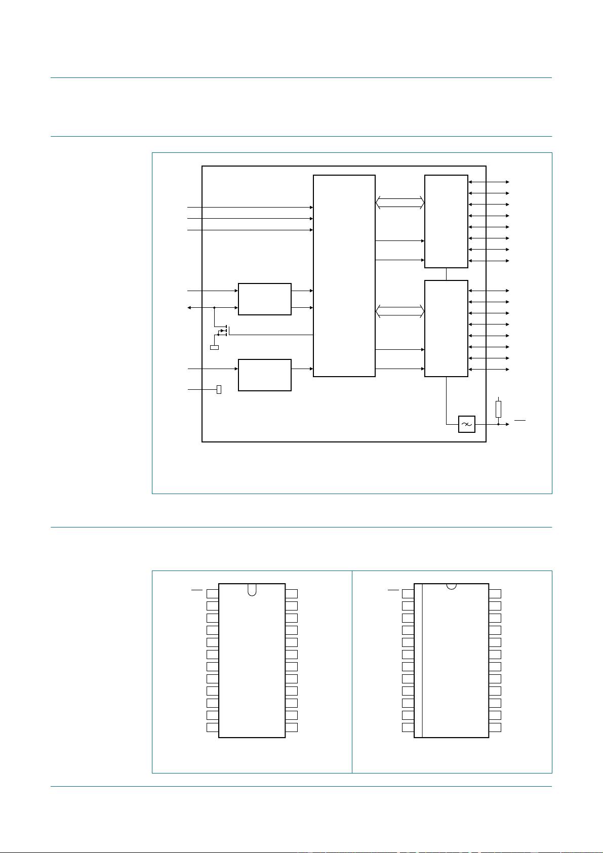
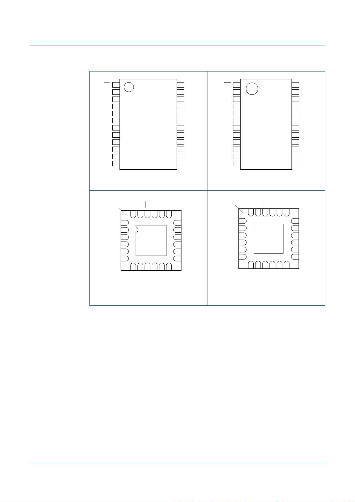
PCA9555
16-bit I
2
C-bus and SMBus I/O port with interrupt
Rev. 07 — 5 June 2007 Product data sheet
PCA9555_7 © NXP B.V. 2007. All rights reserved.
Product data sheet Rev. 07 — 5 June 2007 2 of 35
NXP Semiconductors
PCA9555
16-bit I
2
C-bus and SMBus I/O port with interrupt
n Latch-up testing is done to JEDEC Standard JESD78 which exceeds 100 mA
n Six packages offered: DIP24, SO24, SSOP24, TSSOP24, HVQFN24 and HWQFN24
3. Ordering information
3.1 Ordering options
Table 1. Ordering information
Type number Package
Name Description Version
PCA9555N DIP24 plastic dual in-line package; 24 leads (600 mil) SOT101-1
PCA9555D SO24 plastic small outline package; 24 leads;
body width 7.5 mm
SOT137-1
PCA9555DB SSOP24 plastic shrink small outline package; 24 leads;
body width 5.3 mm
SOT340-1
PCA9555PW TSSOP24 plastic thin shrink small outline package; 24 leads;
body width 4.4 mm
SOT355-1
PCA9555BS HVQFN24 plastic thermal enhanced very thin quad flat package;
no leads; 24 terminals; body 4 × 4 × 0.85 mm
SOT616-1
PCA9555HF HWQFN24 plastic thermal enhanced very very thin quad flat
package; no leads; 24 terminals; body 4 × 4 × 0.75 mm
SOT994-1
Table 2. Ordering options
Type number Topside mark Temperature range
PCA9555N PCA9555 −40 °C to +85 °C
PCA9555D PCA9555D −40 °C to +85 °C
PCA9555DB PCA9555 −40 °C to +85 °C
PCA9555PW PCA9555PW −40 °C to +85 °C
PCA9555BS 9555 −40 °C to +85 °C
PCA9555HF P55H −40 °C to +85 °C
PCA9555_7 © NXP B.V. 2007. All rights reserved.
Product data sheet Rev. 07 — 5 June 2007 3 of 35
NXP Semiconductors
PCA9555
16-bit I
2
C-bus and SMBus I/O port with interrupt
4. Block diagram
5. Pinning information
5.1 Pinning
Remark: All I/Os are set to inputs at reset.
Fig 1. Block diagram of PCA9555
PCA9555
POWER-ON
RESET
002aac702
I
2
C-BUS/SMBus
CONTROL
INPUT
FILTER
SCL
SDA
V
DD
INPUT/
OUTPUT
PORTS
IO0_0
V
SS
8-bit
write pulse
read pulse
IO0_2
IO0_1
IO0_3
IO0_4
IO0_5
IO0_6
IO0_7
INPUT/
OUTPUT
PORTS
IO1_0
8-bit
write pulse
read pulse
IO1_2
IO1_1
IO1_3
IO1_4
IO1_5
IO1_6
IO1_7
INT
A1
A0
A2
LP filter
V
DD
Fig 2. Pin configuration for DIP24 Fig 3. Pin configuration for SO24
V
DD
SDA
SCL
A0
IO1_7
IO1_6
IO1_5
IO1_4
IO1_3
IO1_2
IO1_1
IO1_0
INT
A1
A2
IO0_0
IO0_1
IO0_2
IO0_3
IO0_4
IO0_5
IO0_6
IO0_7
V
SS
PCA9555N
002aac697
1
2
3
4
5
6
7
8
9
10
11
12
14
13
16
15
18
17
20
19
22
21
24
23
INT V
DD
A1 SDA
A2 SCL
IO0_0 A0
IO0_1 IO1_7
IO0_2 IO1_6
IO0_3 IO1_5
IO0_4 IO1_4
IO0_5 IO1_3
IO0_6 IO1_2
IO0_7 IO1_1
V
SS
IO1_0
PCA9555D
002aac698
1
2
3
4
5
6
7
8
9
10
11
12
14
13
16
15
18
17
20
19
22
21
24
23
PCA9555_7 © NXP B.V. 2007. All rights reserved.
Product data sheet Rev. 07 — 5 June 2007 4 of 35
NXP Semiconductors
PCA9555
16-bit I
2
C-bus and SMBus I/O port with interrupt
Fig 4. Pin configuration for SSOP24 Fig 5. Pin configuration for TSSOP24
Fig 6. Pin configuration for HVQFN24 Fig 7. Pin configuration for HWQFN24
INT
A1
A2
IO0_0
IO0_1
IO0_2
IO0_3
IO0_4
IO0_5
IO0_6
IO0_7
V
SS
PCA9555DB
002aac699
1
2
3
4
5
6
7
8
9
10
11
12
14
13
16
15
18
17
20
19
22
21
24
23
V
DD
SDA
SCL
A0
IO1_7
IO1_6
IO1_5
IO1_4
IO1_3
IO1_2
IO1_1
IO1_0
V
DD
SDA
SCL
A0
IO1_7
IO1_6
IO1_5
IO1_4
IO1_3
IO1_2
IO1_1
IO1_0
INT
A1
A2
IO0_0
IO0_1
IO0_2
IO0_3
IO0_4
IO0_5
IO0_6
IO0_7
V
SS
PCA9555PW
002aac700
1
2
3
4
5
6
7
8
9
10
11
12
14
13
16
15
18
17
20
19
22
21
24
23
002aac701
PCA9555BS
Transparent top view
IO1_3
IO0_4
IO0_5
IO1_4
IO0_3 IO1_5
IO0_2 IO1_6
IO0_1 IO1_7
IO0_0 A0
IO0_6
IO0_7
V
SS
IO1_0
IO1_1
IO1_2
A2
A1
V
DD
SDA
SCL
terminal 1
index area
6
13
5
14
4 15
3 16
2 17
1
18
7
8
9
10
11
12
24
23
22
21
20
19
INT
002aac881
Transparent top view
IO1_3
IO0_4
IO0_5
IO1_4
IO0_3 IO1_5
IO0_2 IO1_6
IO0_1 IO1_7
IO0_0 A0
IO0_6
IO0_7
V
SS
IO1_0
IO1_1
IO1_2
A2
A1
INT
V
DD
SDA
SCL
terminal 1
index area
6
13
5
14
4 15
3 16
2 17
1
18
7
8
9
10
11
12
24
23
22
21
20
19
PCA9555HF
PCA9555_7 © NXP B.V. 2007. All rights reserved.
Product data sheet Rev. 07 — 5 June 2007 5 of 35
NXP Semiconductors
PCA9555
16-bit I
2
C-bus and SMBus I/O port with interrupt
5.2 Pin description
[1] HVQFN and HWQFN package die supply ground is connected to both the V
SS
pin and the exposed center
pad. The V
SS
pin must be connected to supply ground for proper device operation. For enhanced thermal,
electrical, and board-level performance, the exposed pad needs to be soldered to the board using a
corresponding thermal pad on the board, and for proper heat conduction through the board thermal vias
need to be incorporated in the PCB in the thermal pad region.
Table 3. Pin description
Symbol Pin Description
DIP24, SO24,
SSOP24, TSSOP24
HVQFN24,
HWQFN24
INT 1 22 interrupt output (open-drain)
A1 2 23 address input 1
A2 3 24 address input 2
IO0_0 4 1 port 0 input/output
IO0_1 5 2
IO0_2 6 3
IO0_3 7 4
IO0_4 8 5
IO0_5 9 6
IO0_6 10 7
IO0_7 11 8
V
SS
12 9
[1]
supply ground
IO1_0 13 10 port 1 input/output
IO1_1 14 11
IO1_2 15 12
IO1_3 16 13
IO1_4 17 14
IO1_5 18 15
IO1_6 19 16
IO1_7 20 17
A0 21 18 address input 0
SCL 22 19 serial clock line
SDA 23 20 serial data line
V
DD
24 21 supply voltage
剩余34页未读,继续阅读
laolixue
- 粉丝: 0
- 资源: 16
上传资源 快速赚钱
- 我的内容管理 收起
- 我的资源 快来上传第一个资源
- 我的收益 登录查看自己的收益
- 我的积分 登录查看自己的积分
- 我的C币 登录后查看C币余额
- 我的收藏
- 我的下载
- 下载帮助
会员权益专享
最新资源
- JSBSim Reference Manual
- c++校园超市商品信息管理系统课程设计说明书(含源代码) (2).pdf
- 建筑供配电系统相关课件.pptx
- 企业管理规章制度及管理模式.doc
- vb打开摄像头.doc
- 云计算-可信计算中认证协议改进方案.pdf
- [详细完整版]单片机编程4.ppt
- c语言常用算法.pdf
- c++经典程序代码大全.pdf
- 单片机数字时钟资料.doc
- 11项目管理前沿1.0.pptx
- 基于ssm的“魅力”繁峙宣传网站的设计与实现论文.doc
- 智慧交通综合解决方案.pptx
- 建筑防潮设计-PowerPointPresentati.pptx
- SPC统计过程控制程序.pptx
- SPC统计方法基础知识.pptx
资源上传下载、课程学习等过程中有任何疑问或建议,欢迎提出宝贵意见哦~我们会及时处理!
点击此处反馈
安全验证
文档复制为VIP权益,开通VIP直接复制
信息提交成功
评论2