EZ-USB
®
FX3™ Hardware Design Guidelines and Schematic Checklist
www.cypress.com Document No. 001-70707 Rev. *D 4
voltage falls down to less than 0.83 V for more than
200 ns. The 1.2 V power network must be designed such
that the VDD does not drop below 0.83 V when an inrush
event occurs. Proper combination of decoupling capacitors
(as specified in the datasheet), inductor chokes and
regulator output impedance are required to make this
possible.
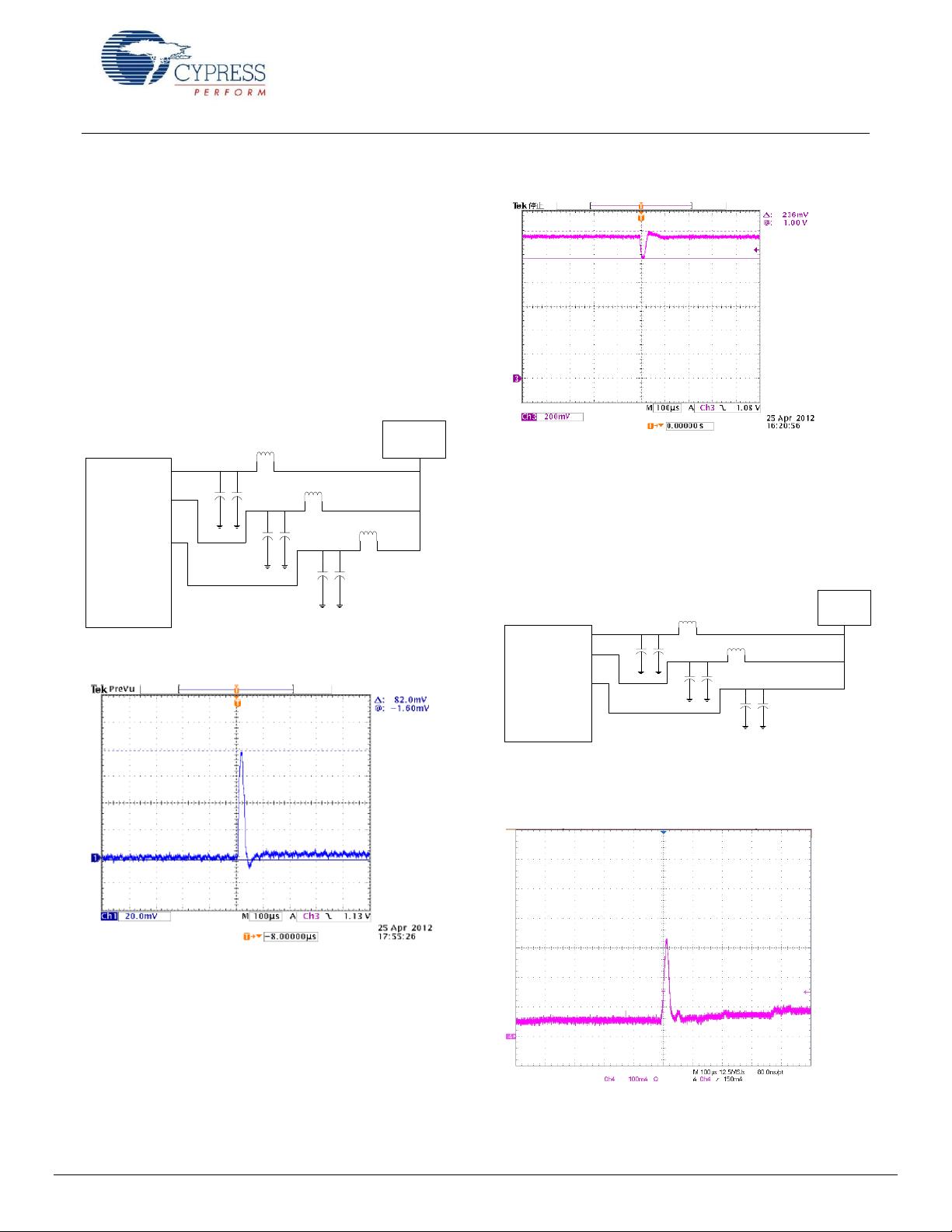
The following example waveforms show the inrush current
(Figure 4) and resultant drop in VDD levels (Figure 5)
when the current spike occurs. The results were obtained
from a non-optimized power supply design using
TPS76801QD power regulator, 2.2 uF decoupling caps
and chokes as shown in Figure 3.
Figure 3. Non-optimized Power Supply Design
U3RXVDDQ
U3TXVDDQ
VDD
FX3
0.1µF 2.2µF
0.1µF 2.2µF
0.1µF 2.2µF
Lchoke
Lchoke
Lchoke
Regulator
TPS76801QD
V1P2
Figure 4. Inrush Current (80 mV/0.1 Ω = 800 mA)
Figure 5. 1.2 V Power Domain Voltage Drop (200 mV)
In contrast, an optimized power design shown in Figure 6
below designed using the same regulator (TPS76801QD),
with the modification of using 22 uF decoupling capacitor
and removing the choke from VDD supply, shows a
reduction in the inrush (Figure 7) and an improvement in
the power supply drop (Figure 8).
Figure 6. Optimized Power Supply Design
U3RXVDDQ
U3TXVDDQ
VDD
FX3
0.1µF 22µF
0.1µF 22µF
0.1µF 22µF
Lchoke
Lchoke
Regulator
TPS76801QD
V1P2
Figure 7. Inrush Current (320 mA)


