LIU et al.: 130-nm FERROELECTRIC NVSoC WITH DIRECT PERIPHERAL RESTORE ARCHITECTURE 891
TABLE II
C
OMPARISON OF REPORTED NVPs
process with a 1.3-V supply voltage for digital logic and a
3.3-V supply voltage for FeRAM, I/O, and analog circuits.
The total die area is 22.09 mm
2
. The NVSoC has 1910 dis-
tributed NVFFs. Two 32-kB FeRAM macros are used as
data memory and instruction memory, respectively. With the
data and instruction FeRAMs turned on, the maximum clock
frequency is 16 MHz, and the active power consumption is
371 μW/MHz. And with the FeRAMs turned off, the clock
frequency is up to 30 MHz, and the NVSoC consumes
234 μW/MHz. In this case, the NVSoC operates from an
instruction cache.
Table II compares the NVSoC with a few silicon verified
NVPs [4]–[11]. The NVSoC has the following advantages.
First, the power management subsystem is integrated on-chip,
which minimizes the number of external components and
hence the form-factor and mass of NVSoC-based IoT devices.
In addition, the reconfigurablility of the supply detection cir-
cuit makes the NVSoC applicable to versatile power sources.
Second, most of the previous NVPs [4]–[6], [8], [10] operate
in two power modes (ACTIVE and
OFF). The NVPs reported
in [9] and [11] add a RETENTION mode to sustain short
power interruptions and reduce the number of backup and
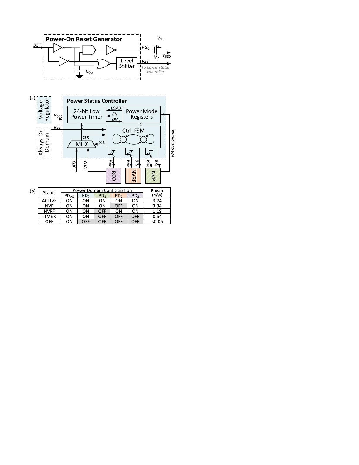
restore operations. In this paper, the NVSoC has five-level
power modes, which support both periodical and energy-driven
applications and provide more flexibility in power manage-
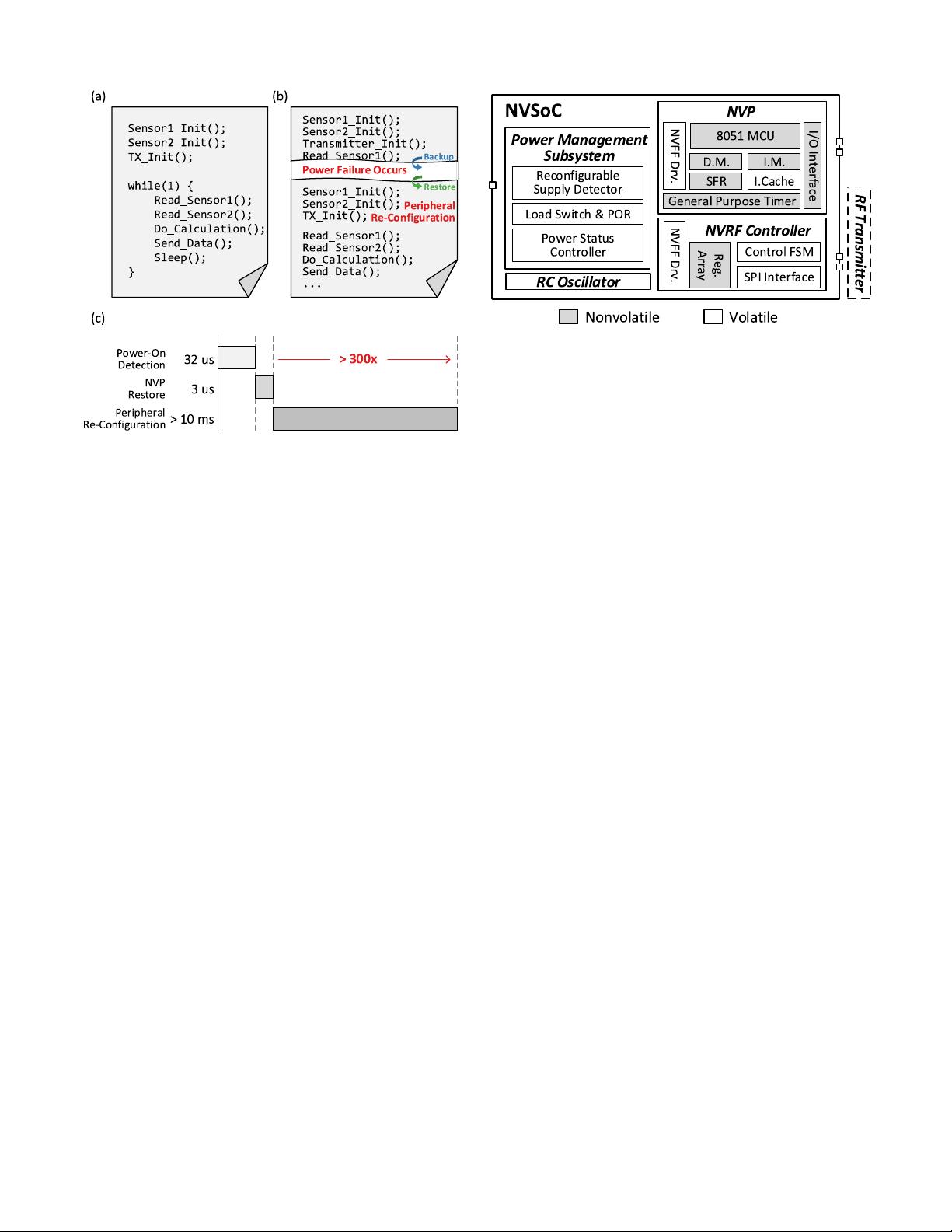
ment strategies. Third, all previous NVPs have to configure the
peripheral devices by software. Instead, this paper features
the direct peripheral restore architecture. It enables parallel
re-configuration of peripheral devices and allows the NVP to
resume its computation task immediately after power resump-
tion. Finally, the NVSoC integrates an instruction cache to
remedy the high power dissipation and limited clock frequency
constrained by the FeRAM. The benefits of the instruction
cache will be discussed in Section V-C.
Table II also compares the active power, startup time,
throughput, and energy efficiency of the NVSoC with pre-
vious NVPs. For a fair comparison, we assume that all of
the NVPs and the NVSoC operate at 8 MHz (which is the
maximum clock frequency of NVP [4]) and perform a typi-
cal sense-compute-transmit task. In this application scenario,
the peripheral devices have 32-byte configuration data in total,
and 4 bytes of data are sensed, averaged, and transmitted.
The throughput and the energy efficiency are defined as how
many sense-compute-transmit tasks are finished within the
same time and with the same amount of energy, respectively.
The power supply is a 100-Hz square wave to emulate the
power failure in energy harvesting systems. The performances
of the previous NVPs [4]–[11] are estimated based on their
micro-architecture and on-chip bus protocol. There are two
reasons that the proposed NVSoC has higher active power than
the previous NVPs [4], [5], [8], which have similar CMOS
technology and NVM. First, the NVRF controller increases the
active power, but it can be turned off after the configuration
and transmission procedure. Second, the level of integration
of the proposed NVSoC is higher, and the clock and power
management subsystems also increase the active power. Nev-
ertheless, the NVSoC still outperforms previous NVPs in
startup speed, efficiency, and throughput. This is because the
NVRF controller has lower time and energy overheads than
the software approach when sending configuration and data
packets to the peripheral devices. In addition, the fine-grained
power management saves average power and thereby increases
the energy efficiency.
B. Measurement Results
Fig. 12(a) shows the operating waveform of the NVSoC
for an
OFF–ON cycle. A square-wave signal with 0–3.3-V
amplitude, 100-Hz frequency, and 90% duty cycle is applied
as a power source to emulate the power failures in an energy
harvesting scenario. To verify successful data backup and
restore operations, the NVSoC runs a counter program, and
the counter value is measured through GPIO.Awireless
transceiver ML7266 is connected to the NVSoC via SPI
interface, of which the waveform is captured to measure the
re-configuration time after power resumption. As Fig. 12(a)
shows, the counter value changes from 0 × 46 to 0 × 00
during the power failure period because the supply voltage
drops to zero. And after the power is resumed, the counter
value is restored to 0 × 46. The waveforms of MOSI and
SCLK show that the system-level wake-up procedure (includ-
ing the re-configuration of the transmitter) takes 1.23 ms.
Fig. 12(b) and (c) shows the backup and restore operations.


