没有合适的资源?快使用搜索试试~ 我知道了~
首页MMA8452低功耗三轴加速度传感器:12位分辨率与智能功能
MMA8452是一款由Freescale Semiconductor设计的高性能、低功耗三轴加速度传感器。这款智能传感器的核心特性在于其12位分辨率,这使得它在测量加速度时具有极高的精度。该设备集成了多种嵌入式功能,允许用户进行灵活的配置,包括连接到两个可编程中断引脚,从而显著节省系统能耗。通过这种方式,主机处理器无需持续地轮询数据,而是能够在事件发生时被唤醒,实现了节能。 MMA8452内置了一款FIFO(First-In-First-Out)缓冲器,可以存储多达32个样本的数据,包括X、Y和Z三个轴的12位或8位数据,根据需要可以选择更快的下载速率。这种设计极大地提高了数据处理效率,特别是在分析手势识别和执行用户自定义算法时,避免了在共享I2C总线上传输数据时可能造成的数据丢失问题。此外,FIFO还支持系统级别的节能,当应用程序处理器在数据记录期间处于休眠状态时,能够节省高达96%的总功率消耗。 传感器提供两种滤波选项,即低通滤波和高通滤波,这有助于减少对快速冲击检测和快速运动响应的分析需求,优化数据处理流程。用户可以根据应用需求选择±2g、±4g或±8g的全量程范围,进一步定制传感器的行为。更重要的是,MMA8452允许通过配置嵌入式功能来生成唤醒中断信号,这样传感器可以在监测到特定事件时从低功耗模式切换,确保在不活跃期间仍能保持对环境变化的实时感知。 MMA8452是一款高度灵活且能有效管理能源消耗的三轴加速度传感器,适用于各种需要精确加速度测量并注重低功耗的应用场景,如移动设备、物联网设备以及工业自动化系统等。
资源详情
资源推荐
Sensors
Freescale Semiconductor 10
MMA8450Q
3 Terminology
3.1 Sensitivity
Sensitivity describes the gain of the sensor and can be determined by applying a g acceleration to it, such as the earth's
gravitational field. The sensitivity of the sensor can be determined by subtracting the -1g acceleration value from the +1g
acceleration value and dividing by two.
3.2 Zero-g Offset
Zero-g Offset describes the deviation of an actual output signal from the ideal output signal if no acceleration is present. A
sensor in a steady state on a horizontal surface will measure 0g in X-axis and 0g in Y-axis whereas the Z-axis will measure 1g.
The output is ideally in the middle of the dynamic range of the sensor (content of OUT registers 0x00, data expressed as 2's
complement number). A deviation from ideal value in this case is called Zero-g offset. Offset is to some extent a result of stress
on the MEMS sensor and therefore the offset can slightly change after mounting the sensor onto a printed circuit board or
exposing it to extensive mechanical stress.
3.3 Self-Test
Self-Test checks the transducer functionality without external mechanical stimulus. When Self-Test is activated, an
electrostatic actuation force is applied to the sensor, simulating a small acceleration. In this case the sensor outputs will exhibit
a change in their DC levels which are related to the selected full scale through the device sensitivity. When Self-Test is activated,
the device output level is given by the algebraic sum of the signals produced by the acceleration acting on the sensor and by the
electrostatic test-force.
4 Modes of Operation
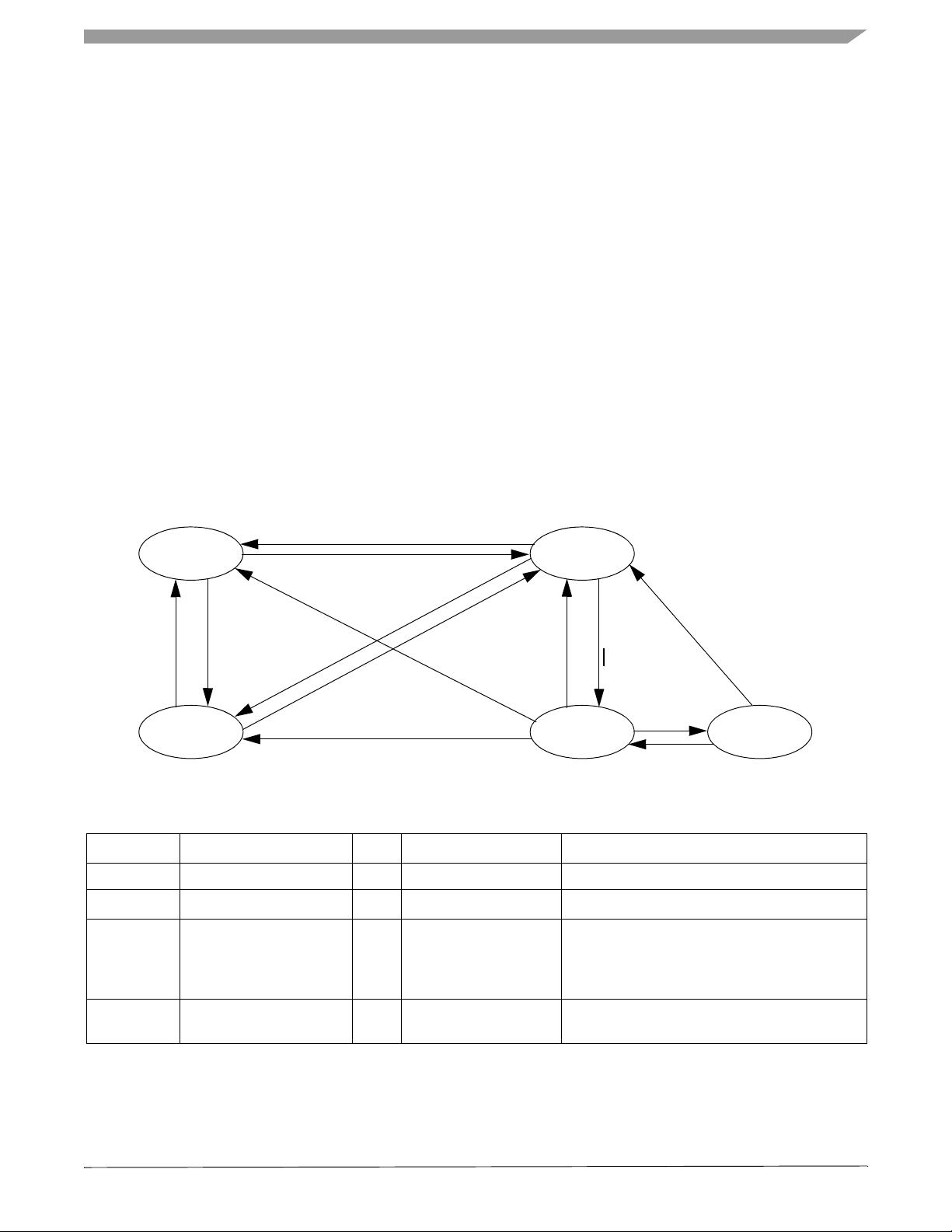
Figure 6. MMA8450Q Mode Transition Diagram
All register contents are preserved when transitioning from Active to Standby mode. Some registers are reset when
transitioning from Standby to Active. These are all noted in the device memory map register table. For more detail on how to use
the Sleep and Wake modes and how to transition between these modes, please refer to the functionality section of this document.
Table 7. Mode of Operation Description
Mode
I
2
C Bus State
VDD EN Function Description
OFF
Powered Down <1.5 V <VDD + 0.3 V The device is powered off.
SHUTDOWN
I
2
C communication ignored
ON
EN = Low All analog & digital blocks are shutdown.
STANDBY
I
2
C communication possible
ON
EN = VDD
Standby register set
Only POR and digital blocks are enabled.
Analog subsystem is disabled.
Registers accessible for Read/Write.
Device configuration done in this mode.
ACTIVE
I
2
C communication possible
ON
EN = VDD
Standby register reset
All blocks are enabled (POR, digital, analog).
VDD = OFF
Mode
SHUTDOWN
Mode
STANDBY
Mode (00)
WAKE
Mode (01)
OFF
E
N
=
V
D
D
E
N
=
GN
D
EN = GND
V
D
D
=
O
F
F
FS = 0
EN = GND
VDD = OFF
VDD = ON
SLEEP
Mode (10)
EN = VDD & VDD = ON
Sensors
Freescale Semiconductor 11
MMA8450Q
5Functionality
The MMA8450Q is a low-power, digital output 3-axis linear accelerometer packaged in a QFN package. The complete device
includes a sensing element and an IC interface able to take the information from the sensing element and to provide a signal to
the external world through an I
2
C serial interface. There are many embedded features in this accelerometer with a very flexible
interrupt routing scheme to two interrupt pins including:
• 8-bit or 12-bit data, high pass filtered data, 8-bit or 12-bit configurable 32 sample FIFO
• Low power and Auto-Wake/Sleep for conservation of current consumption
• Single and double pulse detection 1 channel
• Motion detection and Freefall 2 channels
• Transient detection based on a high pass filter and settable threshold for detecting the change in acceleration above a
threshold
• Flexible user configurable portrait landscape detection algorithm addressing many use cases for screen orientation
All functionality is available in 2g, 4g or 8g dynamic ranges. There are many configuration settings for enabling all the different
functions. Separate application notes have been provided to help configure the device for each embedded functionality.
5.1 Device Calibration
The IC interface is factory calibrated for sensitivity and Zero-g offset for each axis. The trim values are stored in Non Volatile
Memory (NVM). On power-up, the trim parameters are read from NVM and applied to the circuitry. In normal use, further
calibration in the end application is not necessary. However, the MMA8450Q allows the user to adjust the Zero-g offset for each
axis after power-up, changing the default offset values. The user offset adjustments are stored in 6 volatile registers. For more
information on device calibration, refer to Freescale application note, AN3916.
5.2 8-bit or 12-bit Data
The measured acceleration data is stored in the OUT_X_MSB, OUT_X_LSB, OUT_Y_MSB, OUT_Y_LSB, OUT_Z_MSB, and
OUT_Z_LSB registers as 2’s complement 12-bit numbers. The most significant 8-bits of each axis are stored in OUT_X (Y,
Z)_MSB, so applications needing only 8-bit results can use these 3 registers and ignore OUT_X(Y, Z)_LSB.
When the full-scale is set to 2g, the measurement range is -2g to +1.999g, and each LSB corresponds to 1g/1024 (0.98 mg)
at 12-bits resolution. When the full-scale is set to 8g, the measurement range is -8g to +7.996g, and each LSB corresponds to
1g/256 (3.9 mg) at 12-bits resolution. The resolution is reduced by a factor of 16 if only the 8-bit results are used. For more
information on the data manipulation between data formats and modes, refer to Freescale application note, AN3922. There is a
device driver available that can be used with the Sensor Toolbox demo board (LFSTBEB8450Q) with this application note.
5.3 Internal FIFO Data Buffer
MMA8450Q contains a 32 sample internal FIFO data buffer minimizing traffic across the I
2
C bus. The FIFO can also provide
power savings of the system by allowing the host processor/MCU to go into a sleep mode while the accelerometer independently
stores the data, up to 32 samples per axis. The FIFO can run at all output data rates. There is the option of accessing the full 12-
bit data for accessing only the 8-bit data. When access speed is more important than high resolution the 8-bit data flush is a better
option.
The FIFO contains three modes (Fill Buffer Mode, Circular Buffer Mode, and Disabled) described in the F_SETUP Register
0x13. Fill Buffer Mode collects the first 32 samples and asserts the overflow flag when the buffer is full. It does not collect anymore
data until the buffer is read. This benefits data logging applications where all samples must be collected. The Circular Buffer Mode
allows the buffer to be filled and then new data replaces the oldest sample in the buffer. The most recent 32 samples will be stored
in the buffer. This benefits situations where the processor is waiting for an specific interrupt to signal that the data must be flushed
to analyze the event.
The MMA8450Q FIFO Buffer also has a configurable watermark, allowing the processor to be interrupted after a configurable
number of samples has filled in the buffer (1 to 32).
For details on the configurations for the FIFO Buffer as well as more specific examples and application benefits, refer to
Freescale application note, AN3920.
5.4 Low Power Mode
The MMA8450Q can be set to a low power mode to further reduce the current consumption of the device. When the Low Power
Mode is enabled, the device has access to all the configurable sampling rates and features as is available in the Normal power
mode. To set the device into Low Power Mode, bit 0 in the System Control Register 2 (0x39) should be set (1) (this bit is cleared
(0) for Normal Power Mode). Low Power Mode reduces the current consumption by internally sleeping longer and averaging the
data less. The Low Power Mode is an additional feature that is independent of the sleep feature.The sleep feature can also be
used to reduce the current consumption by automatically changing to a lower sample rate when no activity is detected.
For more information on how to configure the MMA8450Q in Low Power Mode and the power consumption benefits of Low
Power Mode and Auto-Wake/Sleep with specific application examples, refer to Freescale application note, AN3921.
剩余54页未读,继续阅读
feisikair
- 粉丝: 0
- 资源: 11
上传资源 快速赚钱
- 我的内容管理 展开
- 我的资源 快来上传第一个资源
- 我的收益 登录查看自己的收益
- 我的积分 登录查看自己的积分
- 我的C币 登录后查看C币余额
- 我的收藏
- 我的下载
- 下载帮助
最新资源
- AirKiss技术详解:无线传递信息与智能家居连接
- Hibernate主键生成策略详解
- 操作系统实验:位示图法管理磁盘空闲空间
- JSON详解:数据交换的主流格式
- Win7安装Ubuntu双系统详细指南
- FPGA内部结构与工作原理探索
- 信用评分模型解析:WOE、IV与ROC
- 使用LVS+Keepalived构建高可用负载均衡集群
- 微信小程序驱动餐饮与服装业创新转型:便捷管理与低成本优势
- 机器学习入门指南:从基础到进阶
- 解决Win7 IIS配置错误500.22与0x80070032
- SQL-DFS:优化HDFS小文件存储的解决方案
- Hadoop、Hbase、Spark环境部署与主机配置详解
- Kisso:加密会话Cookie实现的单点登录SSO
- OpenCV读取与拼接多幅图像教程
- QT实战:轻松生成与解析JSON数据
资源上传下载、课程学习等过程中有任何疑问或建议,欢迎提出宝贵意见哦~我们会及时处理!
点击此处反馈
安全验证
文档复制为VIP权益,开通VIP直接复制
信息提交成功