verilog中的移位寄存器的波形
时间: 2024-06-16 14:05:19 浏览: 168

verilog 描述移位寄存器
移位寄存器是一种常见的数字电路元件,用于在Verilog中实现数据的移位操作。根据引用内容,Verilog中有多种移位寄存器的实现方式,包括左移位寄存器、右移位寄存器、串行输入并行输出移位寄存器和并行输入串行输出移位寄存器[^1]。
下面是一个示例,展示了Verilog中左移位寄存器的波形:
```verilog
module left_shift_reg(
input wire clk,
input wire reset,
input wire [7:0] data_in,
output wire [7:0] data_out
);
reg [7:0] reg_data;
always @(posedge clk or posedge reset) begin
if (reset)
reg_data <= 8'b0;
else
reg_data <= {reg_data[6:0], data_in};
end
assign data_out = reg_data;
endmodule
```
在上述示例中,左移位寄存器通过将输入数据data_in左移一位,并将最高位填充为0来实现数据的移位操作。当时钟信号clk上升沿到来时,数据移位操作会被触发。同时,当复位信号reset为高电平时,寄存器的值会被清零。
请注意,这只是左移位寄存器的一个示例,其他类型的移位寄存器的实现方式和波形可能会有所不同。如果您对其他类型的移位寄存器感兴趣,我可以为您提供更多的信息。
阅读全文
相关推荐
最新推荐
4位串入并出移位寄存器
4. 仿真验证:通过仿真工具对移位寄存器进行仿真验证,能够观察到移位寄存器的输出波形图,验证移位寄存器的正确性。 5. 电子电路控制:移位寄存器是一种基本的电子电路组件,能够实现简单的电子电路控制。通过本次...
基于FPGA的FIR数字滤波器设计方案(一)
具体到FIR数字滤波器的模块设计,例如16阶的FIR滤波器,可以在Simulink环境中用Shift Taps移位寄存器模块分解输入信号,然后根据FIR滤波器的算法进行计算。每个移位寄存器负责存储一部分输入数据,与滤波器系数相乘...
Tobit与Probit模型Stata实现代码-最新发布.zip
Tobit与Probit模型Stata实现代码-最新发布.zip
高清艺术文字图标资源,PNG和ICO格式免费下载
资源摘要信息:"艺术文字图标下载"
1. 资源类型及格式:本资源为艺术文字图标下载,包含的图标格式有PNG和ICO两种。PNG格式的图标具有高度的透明度以及较好的压缩率,常用于网络图形设计,支持24位颜色和8位alpha透明度,是一种无损压缩的位图图形格式。ICO格式则是Windows操作系统中常见的图标文件格式,可以包含不同大小和颜色深度的图标,通常用于桌面图标和程序的快捷方式。
2. 图标尺寸:所下载的图标尺寸为128x128像素,这是一个标准的图标尺寸,适用于多种应用场景,包括网页设计、软件界面、图标库等。在设计上,128x128像素提供了足够的面积来展现细节,而大尺寸图标也可以方便地进行缩放以适应不同分辨率的显示需求。
3. 下载数量及内容:资源提供了12张艺术文字图标。这些图标可以用于个人项目或商业用途,具体使用时需查看艺术家或资源提供方的版权声明及使用许可。在设计上,艺术文字图标融合了艺术与文字的元素,通常具有一定的艺术风格和创意,使得图标不仅具备标识功能,同时也具有观赏价值。
4. 设计风格与用途:艺术文字图标往往具有独特的设计风格,可能包括手绘风格、抽象艺术风格、像素艺术风格等。它们可以用于各种项目中,如网站设计、移动应用、图标集、软件界面等。艺术文字图标集可以在视觉上增加内容的吸引力,为用户提供直观且富有美感的视觉体验。
5. 使用指南与版权说明:在使用这些艺术文字图标时,用户应当仔细阅读下载页面上的版权声明及使用指南,了解是否允许修改图标、是否可以用于商业用途等。一些资源提供方可能要求在使用图标时保留作者信息或者在产品中适当展示图标来源。未经允许使用图标可能会引起版权纠纷。
6. 压缩文件的提取:下载得到的资源为压缩文件,文件名称为“8068”,意味着用户需要将文件解压缩以获取里面的PNG和ICO格式图标。解压缩工具常见的有WinRAR、7-Zip等,用户可以使用这些工具来提取文件。
7. 具体应用场景:艺术文字图标下载可以广泛应用于网页设计中的按钮、信息图、广告、社交媒体图像等;在应用程序中可以作为启动图标、功能按钮、导航元素等。由于它们的尺寸较大且具有艺术性,因此也可以用于打印材料如宣传册、海报、名片等。
通过上述对艺术文字图标下载资源的详细解析,我们可以看到,这些图标不仅是简单的图形文件,它们集合了设计美学和实用功能,能够为各种数字产品和视觉传达带来创新和美感。在使用这些资源时,应遵循相应的版权规则,确保合法使用,同时也要注重在设计时根据项目需求对图标进行适当调整和优化,以获得最佳的视觉效果。
管理建模和仿真的文件
管理Boualem Benatallah引用此版本:布阿利姆·贝纳塔拉。管理建模和仿真。约瑟夫-傅立叶大学-格勒诺布尔第一大学,1996年。法语。NNT:电话:00345357HAL ID:电话:00345357https://theses.hal.science/tel-003453572008年12月9日提交HAL是一个多学科的开放存取档案馆,用于存放和传播科学研究论文,无论它们是否被公开。论文可以来自法国或国外的教学和研究机构,也可以来自公共或私人研究中心。L’archive ouverte pluridisciplinaire
DMA技术:绕过CPU实现高效数据传输
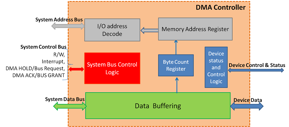
# 1. DMA技术概述
DMA(直接内存访问)技术是现代计算机架构中的关键组成部分,它允许外围设备直接与系统内存交换数据,而无需CPU的干预。这种方法极大地减少了CPU处理I/O操作的负担,并提高了数据传输效率。在本章中,我们将对DMA技术的基本概念、历史发展和应用领域进行概述,为读
SGM8701电压比较器如何在低功耗电池供电系统中实现高效率运作?
SGM8701电压比较器的超低功耗特性是其在电池供电系统中高效率运作的关键。其在1.4V电压下工作电流仅为300nA,这种低功耗水平极大地延长了电池的使用寿命,尤其适用于功耗敏感的物联网(IoT)设备,如远程传感器节点。SGM8701的低功耗设计得益于其优化的CMOS输入和内部电路,即使在电池供电的设备中也能提供持续且稳定的性能。
参考资源链接:[SGM8701:1.4V低功耗单通道电压比较器](https://wenku.csdn.net/doc/2g6edb5gf4?spm=1055.2569.3001.10343)
除此之外,SGM8701的宽电源电压范围支持从1.4V至5.5V的电
mui框架HTML5应用界面组件使用示例教程
资源摘要信息:"HTML5基本类模块V1.46例子(mui角标+按钮+信息框+进度条+表单演示)-易语言"
描述中的知识点:
1. HTML5基础知识:HTML5是最新一代的超文本标记语言,用于构建和呈现网页内容。它提供了丰富的功能,如本地存储、多媒体内容嵌入、离线应用支持等。HTML5的引入使得网页应用可以更加丰富和交互性更强。
2. mui框架:mui是一个轻量级的前端框架,主要用于开发移动应用。它基于HTML5和JavaScript构建,能够帮助开发者快速创建跨平台的移动应用界面。mui框架的使用可以使得开发者不必深入了解底层技术细节,就能够创建出美观且功能丰富的移动应用。
3. 角标+按钮+信息框+进度条+表单元素:在mui框架中,角标通常用于指示未读消息的数量,按钮用于触发事件或进行用户交互,信息框用于显示临时消息或确认对话框,进度条展示任务的完成进度,而表单则是收集用户输入信息的界面组件。这些都是Web开发中常见的界面元素,mui框架提供了一套易于使用和自定义的组件实现这些功能。
4. 易语言的使用:易语言是一种简化的编程语言,主要面向中文用户。它以中文作为编程语言关键字,降低了编程的学习门槛,使得编程更加亲民化。在这个例子中,易语言被用来演示mui框架的封装和使用,虽然描述中提到“如何封装成APP,那等我以后再说”,暗示了mui框架与移动应用打包的进一步知识,但当前内容聚焦于展示HTML5和mui框架结合使用来创建网页应用界面的实例。
5. 界面美化源码:文件的标签提到了“界面美化源码”,这说明文件中包含了用于美化界面的代码示例。这可能包括CSS样式表、JavaScript脚本或HTML结构的改进,目的是为了提高用户界面的吸引力和用户体验。
压缩包子文件的文件名称列表中的知识点:
1. mui表单演示.e:这部分文件可能包含了mui框架中的表单组件演示代码,展示了如何使用mui框架来构建和美化表单。表单通常包含输入字段、标签、按钮和其他控件,用于收集和提交用户数据。
2. mui角标+按钮+信息框演示.e:这部分文件可能展示了mui框架中如何实现角标、按钮和信息框组件,并进行相应的事件处理和样式定制。这些组件对于提升用户交互体验至关重要。
3. mui进度条演示.e:文件名表明该文件演示了mui框架中的进度条组件,该组件用于向用户展示操作或数据处理的进度。进度条组件可以增强用户对系统性能和响应时间的感知。
4. html5标准类1.46.ec:这个文件可能是核心的HTML5类库文件,其中包含了HTML5的基础结构和类定义。"1.46"表明这是特定版本的类库文件,而".ec"文件扩展名可能是易语言项目中的特定格式。
总结来说,这个资源摘要信息涉及到HTML5的前端开发、mui框架的界面元素实现和美化、易语言在Web开发中的应用,以及如何利用这些技术创建功能丰富的移动应用界面。通过这些文件和描述,可以学习到如何利用mui框架实现常见的Web界面元素,并通过易语言将这些界面元素封装成移动应用。
"互动学习:行动中的多样性与论文攻读经历"
多样性她- 事实上SCI NCES你的时间表ECOLEDO C Tora SC和NCESPOUR l’Ingén学习互动,互动学习以行动为中心的强化学习学会互动,互动学习,以行动为中心的强化学习计算机科学博士论文于2021年9月28日在Villeneuve d'Asq公开支持马修·瑟林评审团主席法布里斯·勒菲弗尔阿维尼翁大学教授论文指导奥利维尔·皮耶昆谷歌研究教授:智囊团论文联合主任菲利普·普雷教授,大学。里尔/CRISTAL/因里亚报告员奥利维耶·西格德索邦大学报告员卢多维奇·德诺耶教授,Facebook /索邦大学审查员越南圣迈IMT Atlantic高级讲师邀请弗洛里安·斯特鲁布博士,Deepmind对于那些及时看到自己错误的人...3谢谢你首先,我要感谢我的两位博士生导师Olivier和Philippe。奥利维尔,"站在巨人的肩膀上"这句话对你来说完全有意义了。从科学上讲,你知道在这篇论文的(许多)错误中,你是我可以依
【数据传输高速公路】:总线系统的深度解析
# 1. 总线系统概述
在计算机系统和电子设备中,总线系统扮演着至关重要的角色。它是一个共享的传输介质,用于在组件之间传递数据和控制信号。无论是单个芯片内部的互连,还是不同设备之间的通信,总线技术都是不可或缺的。为了实现高效率和良好的性能,总线系统必须具备高速传输能力、高效的数据处理能力和较高的可靠性。
本章节旨在为读者提供总线系统的初步了解,包括其定义、历史发展、以及它在现代计算机系统中的应用。我们将讨论总线系统的功能和它在不同层